


- News
19 October 2016
Photo-electro-chemical lift-off of free-standing gallium nitride
University of California Santa Barbara (UCSB) in the USA has used photo-electro-chemical (PEC) etch to lift-off c-plane free-standing gallium nitride (GaN) from light-emitting diode (LED) structures as part of a thin-film flip-chip fabrication process [David Hwang et al, Optics Express, vol. 24, p22875, 2016].
The team sees PEC lift-off as an alternative to laser-based techniques. "PEC lift-off causes no damage to the devices, is a batch process as all LEDs are undercut at the same time, is compatible with free-standing GaN substrates, and enables substrate reuse," the researchers write. By contrast, laser lift-off of sapphire growth substrates is a slow chip-by-chip process and has the potential to cause cracking of the LEDs, reducing yield. The laser technique cannot be used for LEDs on free-standing GaN or silicon carbide growth substrates.
Flip-chip orientations for LED fabrication give high light extraction, improved heat extraction, and decreased current crowding. LED performance degrades where there is increased temperature and/or current density.
Using free-standing growth substrates can improve performance by reducing dislocation densities in the light-emitting material, increasing efficiency. However, free-standing GaN substrates are extremely expensive, and reuse should reduce potential production costs. For ultraviolet LEDs, GaN material absorbs the radiation generated and must be removed.
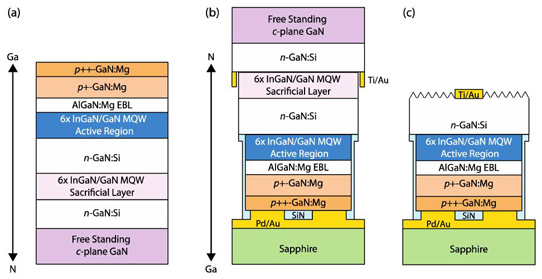
Figure 1: Cross-sectional schematic of (a) as-grown epitaxial structure, (b) partially processed sample after wafer-bonding and before PEC etching, and (c) completely processed sample with p-GaN down and N-face of n-GaN up.
The free-standing c-plane GaN used by UCSB was supplied by Sciocs Company Ltd. The epitaxial structure was grown by metal-organic chemical vapor deposition (Figure 1).
The sacrificial layer consisted of a 6-period multiple quantum well (MQW) of 2.5nm InGaN separated by 7nm GaN barriers, grown on 1.5μm n-GaN. The structure had a 430nm wavelength photoluminescence peak.
The LED part of the structure contained a 3μm n-GaN contact, another 6x(2.5nm/7nm) MQW with emission at 440nm, a 10nm p-AlGaN electron-blocking layer (EBL), a 110nm p+-GaN contact, and a 20nm p++-GaN contact.
Fabrication began with plasma mesa etch down to the n-GaN contact layer above the sacrificial MQW. The sidewalls of the mesa were covered by plasma-enhanced chemical vapor deposition (PECVD) of silicon nitride that protected the LED structure during the photo-electro-chemical etch. Palladium/gold metals were electron-beam evaporated onto the p-GaN contact. The top gold also provided a bonding pad for the flip-chip assembly process.
The sacrificial region was prepared by another plasma etch to expose the sidewalls of the respective MQW structure outside the area defined by the 0.1mm2 LED mesa. A titanium/gold electrode was deposited on the 1.5μm n-GaN as a cathode for the photo-electro-chemical etch.
The structure was flipped and bonded onto sapphire coated with titanium/gold. Then the photo-electro-chemical etch was carried out with backside illumination and potassium hydroxide solution for five hours. The light source was an array of 405nm LEDs. After the free-standing GaN substrate was removed, the n-electrode of titanium/gold was deposited.
The PEC etch proceeds by the holes from electron-hole photo-generation reacting with the potassium hydroxide solution, oxidizing the sacrificial MQW. The titanium/gold electrode extracted the excess electrons into the solution.
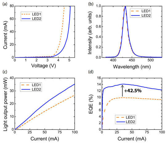
Figure 2: (a) Current-voltage curve for LEDs 1 and 2 after flip-chip processing: 1mA of current corresponds to current density of 1A/cm2. (b) Electroluminescence spectra showing peak wavelength. (c) Dependence of light output power on current. (d) Dependence of EQE on current.
Some of the resulting devices were further etched in potassium hydroxide solution without illumination to further roughen the emission surface, improving light extraction efficiency. Without the extra etch there was still some unintentional roughening from the PEC lift-off etch.
The devices were packaged by dicing, mounting on silver headers, wire-bonding, and encapsulating in 1.4-refractive index silicone.
An LED without extra surface roughening (LED 1) had a 3.5V turn-on, while an LED with roughening (LED 2) had a higher turn-on. The researchers believe this was due to variations in growth across the wafer. The LED 2, however, had much improved light output – 14.6mW output power and 14.1% external quantum efficiency (EQE) at 36A/cm2 current density, compared with 10.3mW and 9.9% for LED 1 (Figure 2). "Roughening resulted in a 42% improvement in output power and EQE," the team writes. The 432nm emission peaks of the devices were similar with full-width at half maximum (FWHM) of 15nm.
In absolute terms there needs to be improvement in output power and EQE. The team suggests that this could be addressed through growth optimizations, incorporating a reflective silver-based p-contact to improve extraction efficiency, and a high thermal conductivity silicon carbide submount to improve heat extraction.
Photo-electro-chemical etch C-plane free-standing GaN LEDs
http://dx.doi.org/10.1364/OE.24.022875
The author Mike Cooke is a freelance technology journalist who has worked in the semiconductor and advanced technology sectors since 1997.


