


- News
24 October 2016
Indium phosphide on silicon template for optoelectronics
Sophia University in Japan has developed a wafer bonding process that produces a thin layer of indium phosphide (InP) on silicon (Si) template that was used for the production of ~1.2μm-wavelength laser diodes (LDs) by metal-organic vapor phase epitaxy (MOVPE) [Keiichi Matsumoto et al, Jpn. J. Appl. Phys., vol55, p112201, 2016].
The team comments: "Although the growth of active materials on an InP/Si substrate was carried out by Morral et al in 2003, the optical property of the as-grown structure was unsatisfactory, and the integration of optical devices has never been demonstrated to our knowledge."
The researchers hope to overcome the limitations of monolithic integration of III-V materials and hybrid bonding of III-V devices onto silicon platforms. Monolithic integration suffers from the generation of anti-phase domains and large lattice mismatches (~8% for InP on Si) giving crystal dislocations and residual strain. Hybrid integration needs high-precision alignment, which is difficult to achieve at low cost.
The Sophia team believes its integration technique could provide the needed light source for optical interconnections on silicon platforms. Silicon photonics waveguides need light with wavelengths longer than 1.1μm.
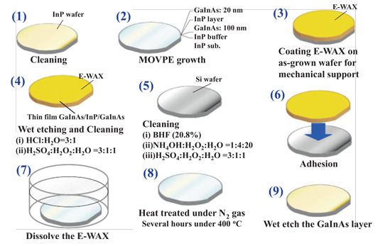
Figure 1: Schematic of InP/Si fabrication process.
The researchers prepared a 2-inch-diameter 1μm-thick InP layer on a silicon wafer through hydrophillic bonding. The process (Figure 1) involved low-pressure MOVPE of gallium indium arsenide (GaInAs) and InP layers on an InP substrate. The buried GaInAs layer functioned as an etch-stop for removal of the original InP substrate.
The team found that ramping the temperature over a period of 45 hours before the final anneal at 400°C decreased the void occupancy rate from more than 3.9% (15-minute ramp) to less than 0.1%. The long ramp time is thought to encourage gas diffusion from the Si/InP interface, avoiding the build up of high internal pressures that create voids. "Thus, we successfully fabricated a void-free 2-inch InP/Si substrate without forming any outgassing channels," the team writes.
The annealing was found to provide an ohmic contact between the InP and Si, compared with the Schottky contact of unannealed samples. Annealing at a higher temperature of 630°C was found to reduce the interface resistance. The 630°C temperature is typical of what is used in MOVPE growth of GaInAs.
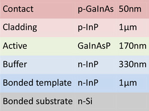 Figure 2: Laser diode layer structure.
The specific resistance of the 630°C interface was between 0.06Ω-cm2 and 0.28Ω-cm2, compared with the range 0.06–0.38Ω-cm2 for 400°C. The current density was 2A/cm2. The researchers claim that the 630°C value is almost the same as for a silicon reference.
Photoluminescence from multiple quantum wells of low-pressure MOVPE GaInAs was almost the same on InP/Si and pure InP substrates in terms of intensity, peak position and full-width at half maximum. X-ray analysis further suggested no degradation of crystal quality from using InP/Si, according to the team.
Finally, the team produced double-heterostructure laser diodes (LDs) with a Ga0.25In0.75As0.45P0.55 active region (Figure 2). The LD wafer was lapped down to 100μm thickness and cleaved into Fabry–Perot bars. The electrodes were gold-zinc on the p-AlGaAs contact layer and gold-aluminium on the n-Si underside. The cavity length was 340μm and the width was 70μm.
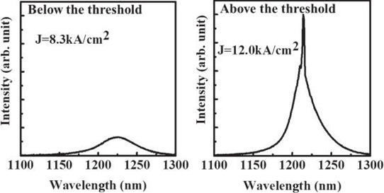
Figure 3: Comparison of laser diode spectra below (a) and above (b) threshold current density.
Under 10kHz 100ns pulses, the threshold current density was 6.4–8.4kA/cm2 at room temperature (Figure 3). A similar device produced on pure InP had a much lower threshold of 3.7kA/cm2.
The researchers comment: "This may be mainly due to heating and less carrier injection owing to an unstable heterointerface. Thus, further investigation of the different characteristics between the LDs on the InP/Si substrate and that on an InP substrate is still required and we hope to report improved LD operation in the future."
InP on Si template InP Laser diodes MOVPE
http://doi.org/10.7567/JJAP.55.112201
The author Mike Cooke is a freelance technology journalist who has worked in the semiconductor and advanced technology sectors since 1997.


