


- News
14 October 2016
Silicon monoxide passivation for gallium nitride transistors
Shandong University in China and University of Manchester in the UK have reported room-temperature thermal-evaporation silicon monoxide (SiO) passivation for aluminium gallium nitride (AlGaN) barrier high-electron-mobility transistors (HEMTs) [Gengchang Zhu et al, Appl. Phys. Lett., vol109, p113503, 2016].
The passivation reduced leakage currents and increased breakdown voltages compared with unpassivated and silicon nitride (SiNx) passivated devices. The researchers comment: "Because of the good passivation effectiveness, no ion damage, simple preparation technology, and low cost, the thermally evaporated SiO is a promising candidate as a surface passivation for GaN-based HEMTs, especially for high-power and noise-sensitive applications."
The SiNx passivation reference was produced using 300°C plasma-enhanced chemical vapor deposition (PECVD), which can suffer from ion damage. "Compared with PECVD and other techniques, thermal evaporation has many advantages such as no ion damage, technical simplicity, and low cost," the researchers claim.
Although the team mentions avoiding current collapse under pulsed current operation as a motivation for passivation, the paper does not report any measurements that would be needed to assess that effect.
SiO has a higher dielectric constant of 5.0 compared with silicon dioxide's 3.9. The breakdown field of both these silicon oxides is around 10MV/cm. Although thermally evaporated SiO has been assessed for use with other technologies such as thin-film transistors, the researchers say that very little work has been carried out on its use in GaN HEMT passivation.
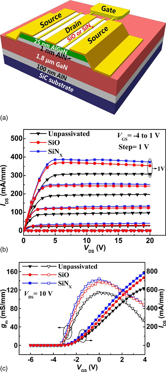
Figure 1: (a) Schematic cross-section of the AlGaN/AlN/GaN HEMTs. (b) Output and (c) transfer characteristics of the unpassivated, SiO-passivated, and SiNx-passivated AlGaN/AlN/GaN HEMTs.
The device material was grown on 6H polytype silicon carbide (SiC), using metal-organic chemical vapor deposition (Figure 1). The conducting two-dimensional electron gas (2DEG) near the GaN/barrier interface had 1.05x10¹³/cm2 sheet carrier density, 298Ω/square sheet resistance, and 1810cm2/V-s carrier mobility (μn), according to Hall measurements.
Device fabrication created plasma-etch mesa isolation, annealed/alloyed titanium/aluminium/nickel/gold source-drain ohmic contacts, nickel/gold gate, 100nm SiO passivation, and plasma-etch contact-pad opening.
The placing of the 2μm-long gate in the 13μm source-drain gap gave a gate-drain distance of 6μm. The gate width was 100μm.
Passivation with SiO, and the SiNx reference, increased Hall sheet carrier density but reduced mobility (Table 1). The researchers suggest that the reduction in mobility could be related to increased Coulomb scattering due to the increased carrier density. The product of carrier density and mobility is higher for the passivated samples. The SiNx has a marginally higher product than SiO passivation.
Table 1: Summary of measurements.
| Sample | Unpassivated | SiO | SiNx |
| ns [1013/cm2] | 1.05 | 1.25 | 369 |
| μn [cm2/V-s] | 1810 | 1.32 | 385 |
| IDmax [mA/mm] | 309 | 1760 | 137 |
| gm [mS/mm] @ VDS = 10V | 116 | 1690 | 144 |
| Ioff [mA/mm] @ VGS = -5V | 2.0x10⁻³ | 2.1x10⁻⁴ | 3.0x10⁻¹ |
| Ion/Ioff | 1.5x10⁵ | 1.8x10⁶ | 1.3x10³ |
| SS [mV/decade] | 181 | 95 | 447 |
| Dit [1012/cm2-eV] | 3.76 | 1.16 | 11.30 |
| Ig [mA/mm] @ VGS = -5V | 3.3x10⁻³ | 3.3x10⁻⁴ | 4.1x10⁻² |
| n | 1.77 | 1.75 | 1.83 |
| ΦB [eV] | 0.79 | 0.85 | 0.73 |
| Vb [V] @ VGS = -5V | 175 | 206 | 111 |
| fT [GHz] @ VDS = 10V, VGS = 0V | 4.0 | 5.2 | 5.8 |
The performance in terms of maximum drain current (IDmax) and transconductance (gm) at 10V drain bias (VDS) on the HEMTs is again better for the passivated devices, with SiNx passivation giving better results. The current and transconductance improvements were, respectively, 19% and 18% for SiO, and 25% and 24% for SiNx. The researchers attribute the improvement to the increased carrier density-mobility product.
However, the SiO passivation has subthreshold and Schottky characteristics that significantly improve on both the unpassivated and SiNx-passivated devices – that is, lower off-current (Ioff), higher on/off current ratio (Ion/Ioff), lower subthreshold swing (SS), lower gate leakage (Ig), and higher Schottky barrier height (ΦB). The SiO passivation also gives the lowest ideality factor (n) for the Schottky diode gate.
The interface trap density (Dit) is also lower for SiO passivation. The researchers comment: "The increased density of interface traps for the SiNx-passivated HEMTs is probably caused by the ion bombardment during the PECVD process, which can be avoided by applying the thermally evaporated SiO."
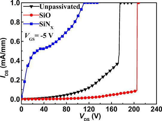
Figure 2: Off-state breakdown characteristics of unpassivated, SiO-passivated, and SiNx-passivated AlGaN/AlN/GaN HEMTs.
Another improvement of SiO passivation is for breakdown voltage (Vb) with -5V gate (VGS), giving the 'off' state. Breakdown was defined at 10-4A drain leakage. The breakdown current was set at a level that did not destroy the devices. The high Vb is claimed to be the result of lower gate leakage and off-current for the SiO passivation.
The SiNx passivation gives a higher current-gain cut-off (fT), while the performance of the SiO-passivated HEMT is better than the unpassivated device. In other studies, SiNx passivation has variously improved and degraded fT performance. The researchers comment: "The increase of fT for the SiO-passivated and the SiNx-passivated HEMTs is attributed to the increased gm and decreased overall capacitance of CGD and CGS."
AlGaN HEMTs SiO passivation PECVD
http://dx.doi.org/10.1063/1.4962894
The author Mike Cooke is a freelance technology journalist who has worked in the semiconductor and advanced technology sectors since 1997.


