


- News
5 October 2016
Electrically driven single-photon emission from atomically thin diodes
The UK's University of Cambridge and Japan's National Institute for Materials Science have developed single-photon emission devices using layers of graphene, hexagonal boron nitride (hBN), and transition-metal dichalcogenides (TMDs) [Carmen Palacios-Berraquero et al, Nature Communications, vol7, p12978, 2016]. "These results present the transition-metal dichalcogenide family as a platform for hybrid, broadband, atomically precise quantum photonics devices," the researchers write.
The device consisted of thin layers that together constituted a tunnel junction (Figure 1). The substrate was silicon with a thermal silicon dioxide layer. The device heterostructure consisted of single-layer graphene (SLG), 2-6-layer hBN, and 1-2-layer tungsten diselenide (WSe2) TMD. The layers were exfoliated from respective bulk materials. The TMD was naturally p-doped; it was also the active light-emitting layer. Electrons were injected from the single-layer graphene through the hBN tunnel barrier into the WSe2 for recombination with holes, giving photons. The contacts were chromium/gold.
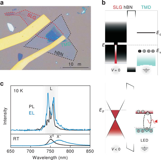
Figure 1: (a) Optical microscope image of typical device. Dotted lines highlight footprints of SLG, hBN and TMD layers. (b) Heterostructure band diagram. Top illustration shows zero-applied bias and bottom finite negative bias applied to the SLG. (c) Example of layered LED emission spectra for optically active layer of WSe2 . Top (bottom) spectra correspond to 10K (room-temperature RT) operation temperature, where black and blue curves are obtained by optical and electrical excitation, respectively.
Photoluminescence (PL) from the structure at room temperature gave a broad peak at 750nm that the researchers associate with the unbound neutral exciton (X0, electron-hole bound state) of WSe2. The peak red-shifts by +20nm in wavelength under electroluminescence (EL). These wavelengths are just outside the visible spectrum (400-700nm) in the infrared (700nm+).
At very low temperature (10K), the spectra blue-shifted by about -30nm due to a slightly wider bandgap. Also, at 10K the spectra show structure, even under EL. The team comments: "In the low-current regime (<1μA for this device) they dominate the EL spectrum, as shown in Fig. 1c, indicating that localized exciton states respond more efficiently to charge injection than the delocalized ones."
Emission from bilayer WSe2 was brighter than the monolayer regions. There were also regions of localized emission bright spots that had a longer wavelength. "These localized states lie within the bandgap of WSe2, and therefore emit at lower energies (longer wavelength) with respect to the bulk exciton emission," the researchers comment.
The linewidths of the localized emitters were between 0.8nm and 3nm. Their distribution density was of the order of 1-2 emitters per 40μm2 of active device area. The positions of the lines from the localized emitters wandered around 2nm over a timescale of seconds.
"Gating and encapsulation of the active layer should aid in reducing the broad linewidths observed here, which we attribute to charge noise in the device," the researchers suggest. "Slow spectral fluctuations can further be reduced through active feedback, for example via the direct current Stark shift."
The team reports that the devices could withstand up to five cooling/heating cycles and several hours of measurement under uninterrupted current.
Hanbury Brown and Twiss interferometer measurements give a low value of 0.29 for the intensity-correlation function (g(2)(0)). Single-photon sources are expected to have values below 0.5. The non-zero value also contains contributions from background emission within a broad spectral window and from dark counts of the detector. The team expects improvements could be made by spectral filtering and optimized charge injection.
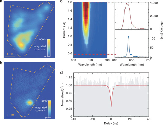
Figure 2: Raster-scan map of integrated EL intensity from monolayer WS2 area: (a) at 0.665μA injection current (bias 2.08V), and (b) at 0.570μA (1.97V). (c) Map of EL spectrum as function of current. Spectrum at the top (bottom) of panel is line cut for injection current of 1.8μA (0.578μA). (d) Intensity-correlation function for localized quantum dot/bright spot in b.
Replacing WSe2 with another TMD, tungsten disulfide (WS2), the researchers found localized red low-temperature (<10K) EL at 640nm with 4nm linewidth with 0.570μA injection. The emission was dominated by single photons, as demonstrated by a g(2)(0) of 0.31 (Figure 2).
The researchers believe that other TMDs could be used as active material. Further a back gate could allow some tuning of the Fermi energy and emission spectrum. They also suggest that couplings with dopant and vacancy levels in silicon or diamond could provide routes to quantum storage and coupling into photonic channels.
www.nature.com/ncomms/2016/160926/ncomms12978/full/ncomms12978.html
The author Mike Cooke is a freelance technology journalist who has worked in the semiconductor and advanced technology sectors since 1997.


