


- News
23 November 2016
Crystal orientation and gallium nitride trench MOSFET performance
University of California, Santa Barbara (UCSB) in the USA and Mitsubishi Chemical Corp in Japan have developed gallium nitride (GaN) trench metal-oxide-semiconductor field-effect transistors (MOSFETs) with different orientations with respect to the crystal structure [Chirag Gupta et al, Appl. Phys. Express, vol9, p121001, 2016]. The devices were oriented nominally in the nonpolar m-plane (1-100) and a-plane (11-20) directions, although the fabrication process was such that the real surfaces of the channel/oxide interface were at an angle to the true GaN crystal planes.
The m-plane devices had better performance compared with the a-plane MOSFETs. In particular, the drain on-current was doubled by orienting the devices with m-planes without increasing the off-current.
Gallium nitride has high critical electric fields for high breakdown voltages along with high mobilities and saturation carrier velocities. Trench MOSFETs are a favorable architecture for reduced on-resistance. High cell density is possible when these transistors are fabricated in hexagonal grids. The crystal structure of gallium nitride is also hexagonal, opening the possibility of performance enhancements through placing the devices in a particular geometric orientation.
The researchers comment: "Understanding the impact of the planes on the channel characteristics is crucial to improving trench-gate device design and performance. However, little is understood since the orientation of hexagonal packed GaN trench-gate MOSFETs has not been disclosed nor discussed in the literature. To the best of our knowledge, these investigations have not yet been pursued."
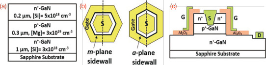
Figure 1: (a) Trench-gate MOSFET epitaxial structure. (b) Hexagonal a- and m-plane-sidewall-oriented devices (top view). (c) Cross-sectional device schematic drawn at dashed lines shown in (b).
The epitaxial material with a p-type layer sandwiched between source-drain n-type layers was grown by metal-organic chemical vapor deposition (MOCVD) on sapphire (Figure 1). The 300nm thickness of the p-type layer constituted the gate length of the devices. Cleaning before the final n-type cap source-contact layer deposition aimed to strip magnesium from the surface, avoiding surface riding of magnesium atoms from the p-type region into the n-type regions. Surface riding refers to a layer of magnesium-rich material on the growth surface of the p-GaN, which can then reduce the effectiveness of subsequent n-type growth with silicon doping.
Fabrication began with trench reactive-ion etching of hexagonal structures aligned variously along the m- and a-plane directions. The taper angle of the trench sidewalls was 81°. The researchers point out that the MOS channel planes were not crystallographically accurate crystal planes.
The samples were cleaned with ultraviolet-ozone and hydrofluoric-acid treatments to remove residual silicon from interfaces. After annealing at 930°C to heal etch damage, the 50nm aluminium oxide (Al2O3) gate dielectric was applied using 700°C MOCVD. Further etching of the source, drain, and body regions was performed to prepare for the titanium/gold source, drain and gate electrodes.
Normal trench MOSFETs have thick lightly doped drift regions to allow higher breakdown voltages to be reached. There was no drift region in the present device structure since its purpose was studying the effect of trench orientation.
The hexagonal structure gave a 180μm gate width. The thresholds of the devices were found to be +9.3V and +9.1V for a- and m-plane orientations, respectively. Positive thresholds imply normally-off behavior, as desired for power applications. However, the thresholds are lower than the +26V predicted by one-dimensional simulations.
"Lowered experimental threshold values compared with estimated values have been observed by other researchers as well and were attributed to sidewall etch damage, which can cause nitrogen vacancies to form and act as donors," the team comments.
There was also some clockwise hysteresis in the threshold voltage value – 0.4V for a- and 0.2V for m-plane MOSFETs.
The on/off current ratios were around 107 for both devices. The subthreshold swing was 480mV/decade for m-plane orientation and 630mV/decade for a-plane orientation. Low values are usually desired for sharp turn-on. Planar device structures can approach the lower theoretical limit of 60mV/decade at room temperature. Devices based on tunneling can go even lower.
The drain current response was higher in the m-plane devices by a factor of about 2 (Figure 2). The researchers estimate the peak channel mobility at 5cm2/V-s for the a-plane MOSFETs and 10cm2/V-s for m-plane devices.
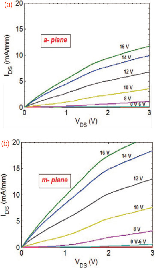
Figure 2: Output drain current-voltage (IDS–VDS) characteristics for (a) a-plane and (b) m-plane-sidewall-oriented trench-gate MOSFETs at applied gate voltage range of 0–16V in steps of 2V.
The team comments: "Further investigations are needed to fully understand the reasons behind the low channel mobility, which could be a result of the fabrication process or fundamental interfacial quality (depending on the gate dielectric used) or both."
Low channel mobility has been an issue for aluminium oxide gate dielectric with planar MOSFETs. Higher channel mobilities have been obtained with silicon nitride or silicon dioxide gate dielectrics.
The team reports "marginal" variations of 10-15% for all performance parameters of the devices.
Other processing factors being equal, the researchers believe the differences in performance between the m- and a-plane MOSFETs could be due to different atom/bond configurations at the sidewall aluminium oxide/non-polar GaN interface. They add: "Higher hysteresis, higher sub-threshold slope, and lower channel mobility together indicate higher trap density and lower interfacial quality in a-plane-oriented devices compared to m-plane-oriented devices.
http://doi.org/10.7567/APEX.9.121001
The author Mike Cooke is a freelance technology journalist who has worked in the semiconductor and advanced technology sectors since 1997.


