


- News
14 November 2016
South Korea's Institute for Basic Science develops thinnest photodetector
By using 2D technology comprising molybdenum disulfide (MoS2) sandwiched in graphene, South Korea's Institute for Basic Science (IBS) Center for Integrated Nanostructure Physics at Sungkyunkwan University (SKKU) has developed what is reckoned to be the world's thinnest photodetector (Woo Jong Yu et al, 'Unusually efficient photocurrent extraction in monolayer van der Waals heterostructure by tunneling through discretized barriers', Nature Communications (2016); DOI: 10.1038/ncomms13278). With a thickness of just 1.3nm (10 times smaller than existing standard silicon diodes) the device could be used in the Internet of Things, smart devices, wearable electronics and photoelectronics.
Graphene is conductive, thin (just one atom thick), transparent and flexible. However, since it does not behave as a semiconductor, its application in the electronics industry is limited. So, to increase graphene's usability, IBS has sandwiched a layer of the 2D semiconductor MoS2 between two graphene sheets and put it over a silicon base. They initially thought that the resulting device was too thin to generate an electric current but, unexpectedly, it did. "A device with one layer of MoS2 is too thin to generate a conventional p-n junction, where positive (p) charges and negative (n) charges are separated and can create an internal electric field. However, when we shine light on it, we observed high photocurrent," says Yu Woo Jong, first author of this study. "Since it cannot be a classical p-n junction, we thought to investigate it further."
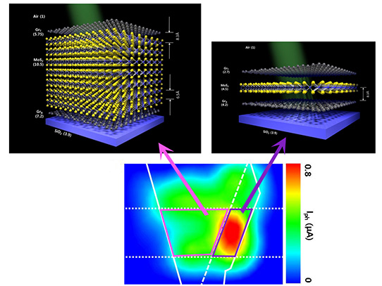
Picture: (top) Devices with one-layer and seven-layer MoS2 were built on top of a silicon base and compared. Dielectric constants responsible for the difference in electrostatic potentials are shown in parenthesis. (bottom) The device with one-layer MoS2 (inside the violet box) showed better performance in converting light to electric current than the seven-layer device (inside the pink box).
To understand what they found, the researchers compared devices with one and seven layers of MoS2 and tested how well they behave as a photodetector, i.e. how they are able to convert light into an electric current. They found that the device with one layer of MoS2 absorbs less light than the device with seven layers, but it has higher photoresponsitivity. "Usually the photocurrent is proportional to the photoabsorbance; that is, if the device absorbs more light, it should generate more electricity, but in this case, even if the one-layer MoS2 device has smaller absorbance than the seven-layer MoS2, it produces seven times more photocurrent," says Yu.
The monolayer is thinner and therefore more sensitive to the surrounding environment. The bottom SiO2 layer increases the energy barrier, while the air on top reduces it, thus electrons in the monolayer device have a higher probability of tunneling from the MoS2 layer to the top graphene (GrT). The energy barrier at the GrT/MoS2 junction is lower than the one at the GrB/MoS2, so the excited electrons transfer preferentially to the GrT layer and create an electric current. Conversely, in the multi-layer MoS2 device, the energy barriers between GrT/MoS2 and GrB/MoS2 are symmetric, therefore the electrons have the same probability to go either side and thus reduce the generated current.
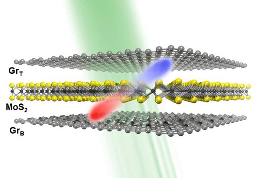
Picture: (a) Device with the MoS2 layer sandwiched between top (GrT) and bottom (GrB) graphene layers. Light (green ray) is absorbed and converted into an electric current. When light is absorbed by the device, electrons (blue) jump into a higher energy state and holes (red) are generated in the MoS2 layer. The movement of holes and electrons created by the difference in electronic potential between the GrT-MoS2 and the GrB-MoS2 junctions generates the electric current.
Yu draws an analogy with a group of people in a valley surrounded by two mountains. The group wants to get to the other side of the mountains, but without making too much effort. In one case (the seven-layers MoS2 device), both mountains have the same height so, whichever mountain is crossed, the effort will be the same. Therefore half the group crosses one mountain and the other half the second mountain.
In the second case (analogous to the one-layer MoS2 device), one mountain is taller than the other, so most of the group decide to cross the smaller mountain. However, because we are considering quantum physics instead of classical electromagnetism, they do not need to climb the mountain until they reach the top (as they would need to do with classical physics), but they can pass through a tunnel. The idea is that electric current is generated by the flow of electrons, and the thinner device can generate more current because more electrons flow towards the same direction.
When light is absorbed by the device and MoS2 electrons jump into an excited state, they leave behind holes (the positive mobile charges that are essentially positions left empty by electrons that absorbed enough energy to jump to a higher energy status). Another problem of the thicker device is that electrons and holes move too slowly through the junctions between graphene and MoS2, leading to their undesired recombination within the MoS2 layer.
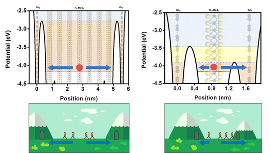
Picture: Mechanism to explain why the device with one-layer MoS2 generates more photocurrent than the seven-layer MoS2 one. (top) In the one-layer device MoS2 (right), the electron (red circle) has a higher probability to tunnel from the MoS2 layer to the GrT because the energy barrier (white arch) is smaller in that junction. In the seven-layers MoS2 device (left) instead, the energy barrier between MoS2/GrT and MoS2/GrB is the same so electrons do not have a preferred direction flow. More energy is generated in the one-layer MoS2 device because more electrons flow in the same direction. (bottom) Imagine that people want to cross a mountain without too much effort. If the mountains have different height (right), more people choose to climb (or better, to tunnel) the small mountain, while if the mountains have the same height (left), they do not have a preferred route. (Graphics modified from Freepiks)
For these reasons, up to 65% of photons absorbed by the thinner device are used to generate a current. Instead, the same measurement (quantum efficiency) is only 7% for the seven-layer MoS2 apparatus.
"This device is transparent, flexible and requires less power than the current 3D silicon semiconductors. If future research is successful, it will accelerate the development of 2D photoelectric devices," Yu believes.
2D transistor made from dual-phase transition-metal dichalcogenide crystal
transition-metal dichalcogenide
www.nature.com/articles/ncomms13278


