


- News
24 May 2016
Wafer-scale lift-off of III-nitride epitaxial layers with boron nitride
Researchers based in USA and France have been studying hexagonal boron nitride (h-BN) as a means to ease wafer-scale separation of III-nitride epitaxial layers from sapphire substrates [Taha Ayari et al, Appl. Phys. Lett., vol108, 171106, 2016]. The team from Georgia Institute of Technology in the USA and its European campus Georgia Tech Lorraine, France, and Université de Lorraine, France, see the technique as potentially having advantages over laser- and chemical-based alternatives for such 'lift-off'.
Hexagonal BN has a crystal structure based on sp2 bonding, which creates strong links in a hexagonal lattice plane but weak van der Waals links between planes. This is similar to a number of material groups such as graphene, black phosphorus, and transition metal dichalcogenides (e.g. molybdenum/tungsten disulfide/diselenide).
Using h-BN, the team believes that problems such as laser damage, long process times and high equipment cost can be ameliorated in epitaxial layer lift-off. Other groups have reported some preliminary results for h-BN lift-off of areas of epitaxial material up to a couple of square centimeters.
The structure (Figure 1) was grown on 2-inch sapphire by metal-organic vapor phase epitaxy (MOVPE). The process precursors were triethylboron (TEB), trimethylgallium/triethylgallium (TMGa/TEG), trimethylindium (TMIn), trimethylaluminum (TMAl), and ammonia (NH3). Doping was achieved by adding silane (SiH4, n-type) and bis(cyclopentadienyl)magnesium (Cp2Mg, p-type).
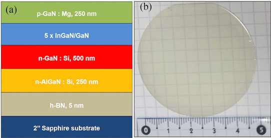
Figure 1: (a) Schematic illustration of grown structure and (b) resulting transparent wafer photograph after epi-growth.
The h-BN layer was grown at 1300°C, followed by aluminium gallium nitride (Al0.14Ga0.86N) at 1100°C as nucleation for the overlying n-GaN. The multiple quantum well (MQW) consisted of five 2.5nm indium gallium nitride (In0.15Ga0.85N) wells separated by 12nm GaN barriers.
The growth of h-BN is described as van der Waals epitaxy (vdWE). The researchers explain: "As opposed to conventional 3D crystals, vdWE does not involve strong chemical bonds between the epilayer and the substrate; instead, it only requires either the substrate or the overlayer to have a surface free of active dangling bonds, such as layered materials which is the case for h-BN."
Atomic force microscopy (AFM) of the p-GaN surface over a 5μmx5μm field gave a root-mean-square (RMS) roughness of 1.6nm.
Separation of the epitaxial layers from the sapphire substrate was attempted using acrylic conductive adhesive on aluminium and copper foils. The exfoliation occurred across the 2-inch wafer with crack-free regions of several square millimeters, according to the researchers. The team comments: "This is greater than the typical device size of commercially available light-emitting diodes (LEDs) (300μmx300μm). We believe that the cracks can be reduced by using a wax support or an elastomeric stamp."
X-ray analysis before and after exfoliation suggested that the MQW stack maintained structural integrity. The RMS roughness was found to be 1.14nm over a 5μmx5μm AFM scan. "This smooth surface indicates that the exfoliation occurred by breaking the bonds between the 2D-layered BN layers and not at the interfaces of the sp3-bonded III-nitride layers which would result in a surface with increased roughness," the researchers write.
Cathodoluminescence (excitation by electron beam) emitted light with an MQW peak at 454nm before exfoliation and 458nm after exfoliation. The researchers attribute the 4nm red-shift to partial residual strain relaxation. The ratio between GaN near band-edge emission and the MQW was the same before and after lift-off, although the overall intensity reduced by about 15%.
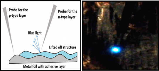
Figure 2: Blue light emission by electrical injection from exfoliated MQW structure.
Electroluminescence was obtained with probe tips, but without contact metal deposition (Figure 2).
Hexagonal boron nitride III-nitride epitaxial layers Sapphire substrates MOVPE
http://dx.doi.org/10.1063/1.4948260
The author Mike Cooke is a freelance technology journalist who has worked in the semiconductor and advanced technology sectors since 1997.


