


- News
29 March 2016
Indium gallium arsenide MOSFET used as radio-frequency switch
Rearchers in China claim the first radio frequency (RF) switch device based on indium gallium arsenide (InGaAs)-channel metal-oxide-semiconductor field-effect transistor (MOSFET) technology [Zhou Jiahui et al, J. Semicond. 2016, vol37, p024005]
Such technology is being developed to boost the performance of present-day complementary metal-oxide semiconductor (CMOS) very-large-scale integrated circuits used in mass-consumer electronics.
RF switches are among the key components in mobile phone wireless communications and GPS systems. Traditionally, these devices have been produced using gallium arsenide high-electron-mobility transistors (HEMTs), although more recently silicon and gallium nitride (GaN) alternatives have been developed.
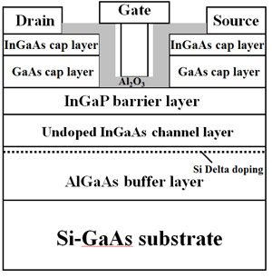 Figure 1: Schematic cross section of In0.4Ga0.6As MOSFET with 10nm Al2O3.
Chinese Academy of Sciences' Institute of Microelectronics and Guilin University of Electronic Technology grew the material for the device (Figure 1) by molecular beam epitaxy (MBE) on semi-insulating GaAs substrate: 300nm aluminium gallium arsenide (Al0.26Ga0.74As) buffer, 7nm In0.4Ga0.6As channel, 5nm indium gallium phosphide (In0.49Ga0.51P) barrier, 50nm n-GaAs cap, and 10nm n-In0.54Ga0.46As cap.
Mesa isolation and channel formation were achieved by wet etching. The structure was cleaned to remove native oxide and excess arsenic before ammonium sulfide passivation.
The aluminium oxide (Al2O3) gate dielectric insulation was applied using atomic layer deposition (ALD). The dielectric was annealed at 400°C in nitrogen. The gate electrode was annealed nickel/gold. The gate length and width were 0.3μm and 300μm, respectively.
The source/drain electrodes were formed by etching away the aluminium oxide and electron-beam evaporation of nickel/germanium/gold/nickel/germanium/gold. A final 300°C anneal completed the fabrication.
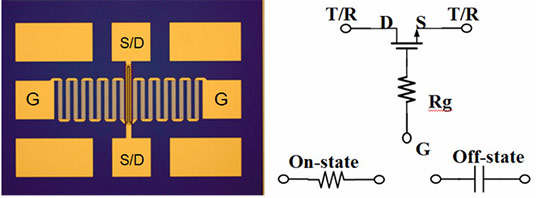
Figure 2: (a) Micrograph of RF switch device. (b) Device equivalent circuit.
To operate as a switch, a gate bias resistor is used to give a circuit (Figure 2) almost equivalent to a two-port device that is a resistor when on and a capacitor when off. The bias resistance needs to be large to isolate the radio-frequency signal.
The MOSFET had a maximum drain current of 250mA/mm and specific turn-on resistance of 0.72Ω-mm2. With 2V drain bias, the maximum transconductance was 370mS/mm with -0.1V gate potential.
The on/off current ratio was about 106 at room temperature with 50mV drain bias, "2–3 orders of magnitude higher than conventional HEMTs," according to the researchers. A subthreshold swing of 220mV/decade was also achieved.
Gate leakage was less than 10-4A/cm2 in the gate potential range of -8V to +7V with 1V drain bias, "3–5 orders of magnitude lower than conventional HEMTs," according to the team.
As an RF switch, the device demonstrated an insertion loss less than 1.8dB in the range 0.1GHz to 10GHz. The minimum was 0.27dB. Isolation was greater than 20dB between 0.1GHz and 7.5GHz with a 68dB maximum. The best performance was achieved at the 0.1GHz end.
The researchers comment: "The insertion loss and isolation of the proposed InGaAs MOSFET switch are 0.27–0.49dB and 35–68dB in the frequency range from 0.1 to 3GHz, which are better than conventional switches."
The handling power of the device was up to 533mW/mm in the on-state and 3667mW/mm in the off-state.
The researchers conclude: "The drain saturation current density and handling power can be improved by increasing the thickness of InGaAs channel. Compared with the conventional GaAs HEMTs, InGaAs MOSFET has a greater potential for RF switches in the future."
http://dx.doi.org/10.1088/1674-4926/37/2/024005
The author Mike Cooke is a freelance technology journalist who has worked in the semiconductor and advanced technology sectors since 1997.


