


- News
8 June 2016
Epitaxial growth of laser diodes on wafer-bonded InP/Si substrates
Sophia University in Japan has developed a technique for growing laser diodes on an indium phosphide (InP) layer bonded to silicon (Si) [Keiichi Matsumoto et al, Appl. Phys. Express, vol9, p062701, 2016]. The researchers claim that this is the first time that an epitaxially grown gallium indium arsenide phosphide/indium phosphide (GaInAsP/InP) double-heterostructure laser diode (LD) has been demonstrated on a wafer-bonded InP/Si substrate. Usually, wafer bonding is performed after the double heterostructure is created.
Although monolithic integration – direct growth of III-V materials on silicon – would be preferred, the technique suffers crystal degradation due to the large lattice mismatch between InP and Si (~8%). On the other hand, wafer bonding suffers from alignment difficulties, making precise high-density integration difficult at low cost.
The researchers comment: "Although the cost of the silicon circuits may be low, the alignment of a prefabricated laser diode chip to a planar optical circuit is time-consuming and expensive, which drives up the cost of the final assembly and packaged device. To solve these problems, we have proposed the monolithic integration of InP-based optical devices on a wafer-bonded InP/Si substrate by low-pressure metal-organic vapor phase epitaxy (MOVPE)."
The InP layer was prepared by growing a GaInAs/n-InP/GaInAs structure on (100) n-InP by MOVPE. The target thickness and carrier concentration of the sandwiched n-InP layer were 1μm and 3x10¹⁸/cm3, respectively. The GaInAs layers functioned as etch-stop layers for the subsequent processing.
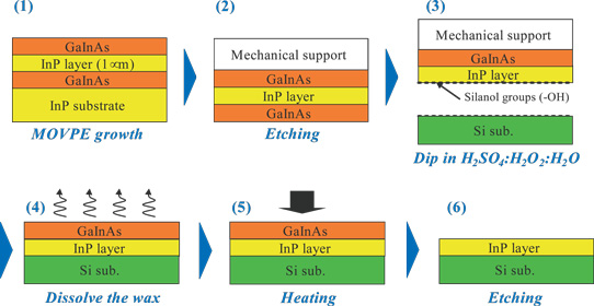
Figure 1: Schematic of InP/Si fabrication process.
A layer of wax was applied to the structure as a mechanical support for the wafer bonding process (Figure 1). The n-InP growth substrate was removed by wet etching. The n-InP and silicon surfaces were cleaned and made hydrophillic before bonding. (It seems, from the paper, that by this stage the GaInAs surface away from the wax support has also been removed during this cleaning process.) The InP and Si surfaces are brought together in deionized water and then dried in a nitrogen gas flow.
The wax support was removed in a warm organic solvent. The n-InP/Si structure is then annealed under top pressure and the final GaInAs layer removed by wet etching.
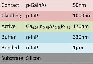
Figure 2: Schematic of grown layer structure.
The double heterostructure for the laser diode was then grown by more MOVPE (Figure 2). Photoluminescence from the structure compared well with that from a structure grown on InP substrate. The researchers say that this indicates negligible degradation of crystal quality from the wafer bonding process.
Laser diodes were fabricated by thinning the wafer to less than 100μm and applying electrodes: gold-zinc to the p-GaInAs topside, and gold-aluminium to the n-Si underside. Laser bars were manually cleaved: 200-300μm long and 50-100μm wide.
A 250μmx90μm device had a threshold current density of 7.5kA/cm2 at room temperature under 10kHz, 100ns pulsed operation. This compares with 3.7kA/cm2 for a device grown on an InP substrate. The researchers point to self-heating, reduced carrier injection due to instability of the heterointerface, and crystalline dark-line defects as leading possible causes of the degraded performance of the device on silicon. Dark-line defects arise from differences in the thermal expansion of InP and silicon.
The researchers suggest that high-reflection coatings could reduce the threshold current.
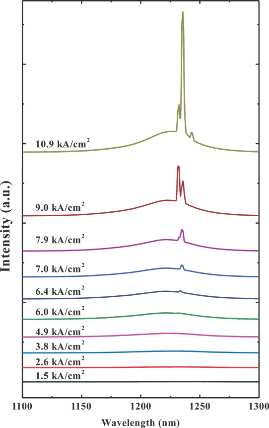
Figure 3: Spectrum at various currents
A kink in the laser output power around 9kA/cm2 is tentatively attributed to lateral-mode lasing due to the slab structure of the device. Spectral analysis showed multiple modes being output as the current increased (Figure 3). "This problem will be overcome by the fabrication of a lateral single-mode waveguide," the team writes.
The researchers conclude: "These results are very promising for the high-density integration of InP-based LDs as light sources for optical interconnection and for overcoming the problems of the conventional hybrid integration approach."
Laser diodes InP Si substrates
http://doi.org/10.7567/APEX.9.062701
The author Mike Cooke is a freelance technology journalist who has worked in the semiconductor and advanced technology sectors since 1997.


