


- News
13 July 2016
Dependence of efficiency droop on carrier density in non-polar samples
The University of Manchester and the University of Cambridge in the UK have been comparing efficiency droop in low-temperature photoluminescence (PL) experiments on non-polar m-plane and polar c-plane indium gallium nitride (InGaN) quantum wells (QWs) [M. J. Davies et al, Appl. Phys. Lett., vol108, p252101, 2016]. The researchers found similar droop behavior in the samples, suggesting that the effect is intrinsically determined by carrier density.
The team comments: "These observations suggest that there is a common mechanism responsible for the efficiency droop, in which delocalized carriers recombine non-radiatively. Our data do not reveal the nature of the non-radiative recombination mechanism, although either Auger recombination or Shockley-Read-Hall recombination at defects is a plausible candidate."
Using non-polar or semi-polar InGaN structures for light-emitting diodes (LEDs) has been found to ease droop in terms of current density. It is usually thought that the reduced efficiency droop in non-polar or semi-polar devices is due to the partial removal of electric fields created by interface charges arising from differences in charge polarization between the various layers of the device. However, some theoreticians at University of California Santa Barbara (UCSB) and University of Michigan have suggested that the carrier density achieved at a certain current density is lower in non-/semi-polar devices, delaying droop onset.
The researchers grew InGaN multiple quantum wells (MQWs) on non-polar m-plane free-standing GaN from wafer company Ammono SA. The wafer was mis-cut 2° towards the (0001) axis. Metal-organic vapor phase epitaxy (MOVPE) was used in a quasi two-temperature process. Five 2.4nm In0.28Ga0.72N wells were grown separated by 6.1nm GaN barriers. The final GaN barrier provided a capping layer. The polar c-plane sample consisted of a single 2.9nm In0.15Ga0.85N well grown using a 750°C single-temperature MOVPE process. Both samples had low-temperature peak emission at ~2.660eV.
The 10K photoluminescence (PL) measurements were carried out with excitation from 100fs (10-13s) 400kHz pulses of 4.881eV photons sourced by a frequency-tripled mode-locked titanium-doped sapphire laser beam. "The use of a pulsed laser, with a pulse duration much shorter than the carrier recombination lifetimes for both samples, ensures that the peak carrier concentration in the QWs is determined by the power density of the excitation source," the researchers comment.
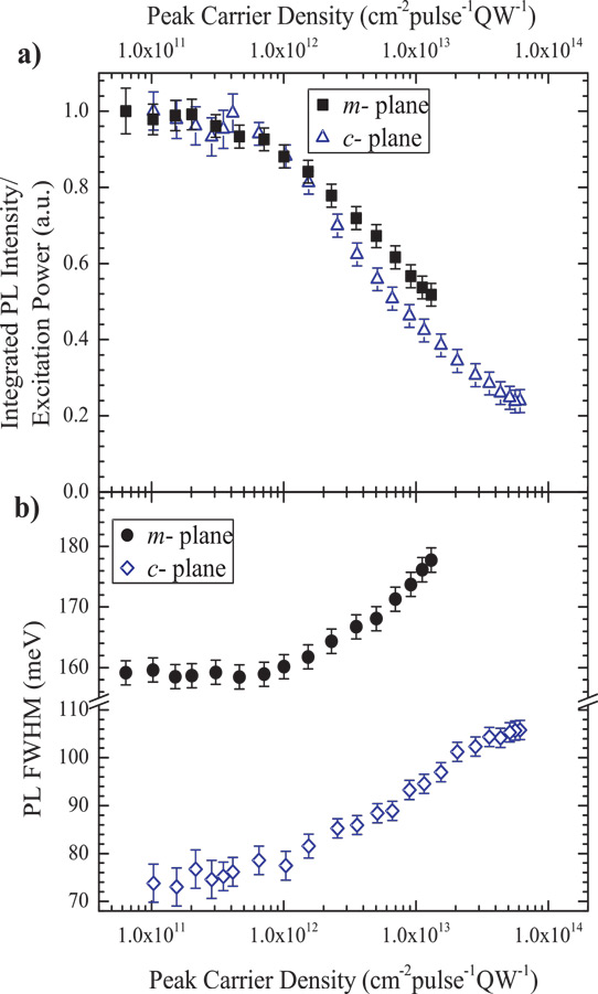
Figure 1: (a) Integrated PL intensity as a function of peak carrier density of m-plane and c-plane samples, measured at 10K, as a function of peak carrier density. (b) FWHM of PL spectra as a function of peak carrier density.
The low-excitation PL peaks for the m- and c-plane samples came at 2.615eV and 2.669eV, respectively. The corresponding full-widths at half maximum (FWHMs) were 158meV and 75meV. The FWHM values remained constant within experimental error until the excitation reached a level where the carrier density in the wells was around 1x10¹²/cm2 per pulse per well (Figure 1). The efficiency in both samples begins to droop around 3x10¹¹/cm2/pulse/well.
Although the carriers were largely created in the GaN layers, given the excitation energy being higher than the ~3.4eV bandgap, the ~2.6eV PL peak led the researchers to "assume that all the carriers are captured by the QW(s); this assumption is supported by the fact that we do not observe a significant amount of recombination from the various GaN layers in the samples." The researchers also believe that in the 5-well m-plane sample, the carriers are evenly distributed between the wells.
The researchers also measured the decay time across the spectra below and above the onset of droop in the m-plane sample (Figure 2). Above the onset, there was a high energy tail in the spectrum, increasing the FWHM. On the low-energy side of the peak, the decay constant remained relatively the same (~260ps) below and above droop onset.
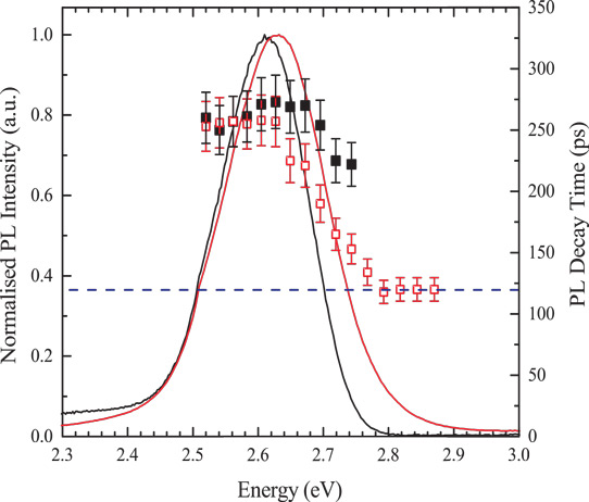
Figure 2: Time-integrated PL spectra for m-plane sample along with PL decay times measured across PL spectrum for peak carrier excitation densities of 1011/cm2/pulse/QW (black line and black data points) and 1.4x10¹³/cm2/pulse/QW (red line and red data points), i.e. measured below and above the onset of efficiency droop. Blue dashed line indicates instrumental time response.
In the non-droop condition with low excitation, there was a slight drop in decay time on the high-energy side of the peak to around 225ps. The team comments: "The origin of this reduction is currently unclear but we suggest that it may be due to the effects of carrier hopping to deeper localized states, as has been observed previously in other localized systems."
For the high excitation droop measurements, the high-side decay constant falls to the instrumental response limit of 120ps. The researchers comment: "The fact the decay constants associated with the main emission band are unchanged at high excitation power densities suggests that the recombination responsible for the main emission band remains purely radiative at the highest carrier densities. This suggests that the new recombination channel on the high-energy side of the spectrum is affected by non-radiative processes that could be responsible for the short decay constant."
The m-plane decay behavior is similar to results of other groups on c-plane samples. In that case, the fast high-energy side decay was attributed to recombination of weakly localized or delocalized carriers when the localized states are saturated. The localization/delocalization of holes seems to be a particularly important precursor for non-radiative losses, giving droop.
Efficiency droop InGaN quantum wells MOVPE
http://dx.doi.org/10.1063/1.4954236
The author Mike Cooke is a freelance technology journalist who has worked in the semiconductor and advanced technology sectors since 1997.


