


- News
25 July 2016
Relaxing multiple quantum wells with low-temperature barriers
South China University of Technology has used low-temperature barriers between indium gallium nitride (InGaN) multiple quantum wells (MQWs) to improve the light output power of light-emitting diodes (LEDs) by 23% to 63.83mW at 65mA [Zhiting Lin et al, Optics Express, vol24, p11885, 2016].
The aim of using low growth temperature was to relax strain in the III-nitride heterostructures. Strain can lead to piezoelectric fields that tend to pull electrons and holes apart, reducing recombination into photons. The researchers hope that their work will lead to increased application of III-nitride LED technology as solid-state lighting (SSL).
The team comments: "Improving the luminous efficiency for LEDs is very important in regard of the energy efficiency and cost efficiency for packaging processes by easing the challenge of heat dissipation, which is the best choice to cope with the large demands from the SSL market. However, the state-of-the-art LEDs are suffering from efficiency droop at high injection current, which has not been fully resolved so far."
The LED material (Figure 1) was grown on c-plane patterned sapphire by metal-organic chemical vapor deposition (MOCVD). The layer thicknesses were: 200nm GaN buffer, 4μm unintentionally doped GaN, 3μm silicon-doped n-GaN, 2nm/6nm 5-period In0.13Ga0.87N/GaN MQW, 3nm/12nm 7-period In0.13Ga0.87N/GaN MQW, 20nm magnesium-doped p-Al0.15Ga0.85N electron-blocking layer (EBL), and 150nm magnesium doped p-GaN.
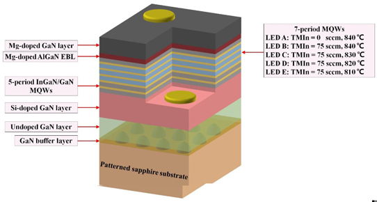
Figure 1: LED structure schemes.
The quantum well layers were all grown at 750°C. However, the barriers for the first 5-period MQW were deposited at 840°C, while the second 7-period MQW barrier were processed at varying temperatures. The first MQW acted as a pre-strained layer over which the second MQW could be grown with reduced biaxial stress.
Most of the barriers in the second MQW also contained indium. Changing the growth temperature of the barriers in the second MQW alters the strain and indium incorporation, as indicated by x-ray diffraction analysis (Table 1). Increased indium incorporation in the barriers reduces the difference in relaxed lattice constant compared with the well. The difference in coefficient of thermal expansion (CTE) is also reduced. This, along with the lower growth temperature, reduces thermally induced stress.
Table 1: Structural parameters of second MQW pairs, FWHMs of −1st satellite peak and relaxation values of wells, R.
Barrier parameters |
Well parameters |
|
|
|||
| Samples | Thickness (nm) | In content | Thickness (nm) | In content | FWHM (arcsec) | R |
| LED A | 12.09 | 0 | 2.92 | 13.14% | 89.78 | 0% |
| LED B | 12.05 | 0.60% | 2.93 | 13.10% | 92.55 | 0.96% |
| LED C | 12.02 | 0.93% | 2.97 | 13.11% | 93.25 | 1.53% |
| LED D | 11.98 | 1.28% | 2.94 | 13.16% | 97.46 | 2.88% |
| LED E | 12.06 | 1.89% | 2.92 | 13.13% | 97.77 | 4.59% |
The materials were fabricated into standard lateral mesa LEDs with 250nm of indium tin oxide (ITO) transparent conductive oxide on the p-GaN top layer and chromium/platinum/gold n- and p-electrodes. The resulting chips were 750μmx220μm.
One effect of lower strain/stress on electroluminescence was found at low current injection, with the lowest-strain device E having a smaller blue-shift of 0.5nm between 2mA and 9mA, compared with 1.7nm for the highest-strain LED A. The researchers attribute this to the reduced quantum-confined Stark effect (QCSE) that arises from strain-dependent piezoelectric fields that become screened with increased current injection.
In terms of power output, the best performance was achieved by the medium-strain LED C (Figure 2). At 65mA current injection, LED C had a boost of 23% over the normal LED A. The forward voltage at 20mA of the devices increased with decreasing strain. The forward voltage values for LEDs A to E were, in order, 3.28V, 3.30V, 3.34V, 3.37V and 3.39V. Higher forward voltage indicates increased resistance and power loss.
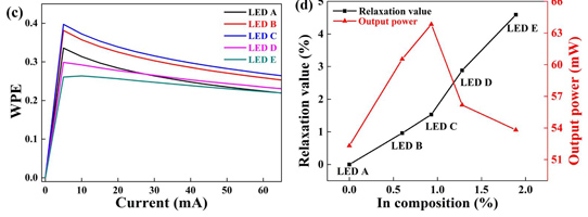
Figure 2: (a) Light output power versus current, (b) current versus voltage and (c) WPE versus current for LEDs A to E; (d) relaxation value of wells and light output power versus indium composition of barriers at 65mA.
The researchers attribute the forward voltage trend probably to degraded crystal quality in the lower-strain devices. Degraded crystal quality can also increase non-radiative recombination of electrons and holes, reducing power output. Increasing full-width at half maximum (FWHM) values for photoluminescence with strain relaxation, from 19.2nm for LED A to 27.8nm for E, also supports the inference of degraded crystal quality in LEDs D and E.
The researchers also determined the wall-plug efficiency (WPE) droop at 65mA for devices A to E to be 34.69%, 33.66%, 33.48%, 22.83% and 15.79%, respectively. "From this result, we can see that the LED with larger relaxation in MQWs owns the weaker WPE droop, which is consistent with the mitigation of the QCSE," the researchers observe. It should also be pointed out that the peak of device E is lower than the other LEDs, making the low droop less impressive.
http://dx.doi.org/10.1364/OE.24.011885
The author Mike Cooke is a freelance technology journalist who has worked in the semiconductor and advanced technology sectors since 1997.


