


- News
19 July 2016
Zirconium dioxide dielectric for gallium nitride high-mobility transistors
The Naval Research Laboratory (NRL) and University of Maryland in the USA claim a record positive threshold voltage of +3.9V for a gallium nitride (GaN) metal-oxide-semiconductor high-electron-mobility transistor (MOS-HEMT) [Travis J. Anderson et al, Appl. Phys. Express, vol9, p071003, 2016]. The team used zirconium dioxide (ZrO2) as a gate dielectric insulator. The positive threshold means that the transistor had normally-off or 'enhancement-mode' operation.
Normally-off transistors are particularly desired in power applications, giving fail-safe operation and more efficient power consumption. The high-power radio frequency (RF) and power switching characteristics of such devices could lead to power amplifier (PA), monolithic microwave integrated circuit (MMIC) and voltage conversion applications.
Using a MOS gate structure significantly reduces gate leakage current, improving reliability and reducing off-state power consumption. ZrO2 has a high dielectric constant of 25, a large bandgap of 7.8eV, and a high breakdown voltage in the range 15-20MV/cm.
The III-nitride heterostructure was grown on high-resistivity silicon with a ~2μm nucleation/transition/GaN-buffer, followed by an 18nm Al0.26Ga0.74N barrier and a 2nm GaN cap. Fabrication began with standard mesa isolation, titanium/aluminium/nickel/gold ohmic metal deposition and annealing, and titanium/gold metal overlay deposition.
Two types of gate were fabricated: a standard Schottky HEMT with nickel/gold gate and plasma-enhanced silicon nitride (PECVD SiNx) passivation; and a MOS-HEMT with full recessing through the AlGaN barrier, 20nm of atomic layer deposition (ALD) ZrO2 gate insulation and a nickel/gold electrode. A ZrO2 MOS-HEMT without recessing was also produced.
The ALD precursors were zirconium(IV) tert-butoxide (ZTB) and deionized water. The researchers comment that no previous ZrO2 GaN MOS-HEMT has used ZTB precursor. Usually, tetrakis(dimethylamino)zirconium is employed. An advantage of ZTB is that its structure already contains some oxygen, which should lead to higher-quality ZrO2 films. The ALD cycle consisted of 0.2-second ZTB and 0.03-second dionized water doses separated by 20-second nitrogen purges, giving ~0.07nm/cycle growth.
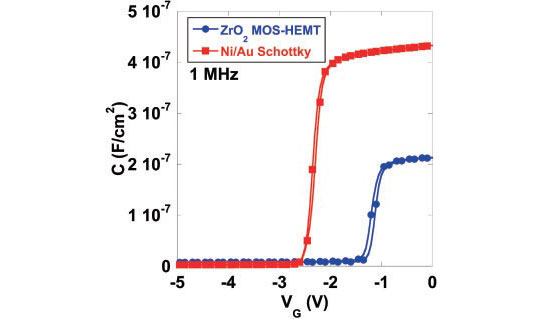
Figure 1: Capacitance–voltage characteristics of Schottky-gated HEMT and ZrO2 MOS-HEMTs.
Capacitance–voltage measurements at 1MHz indicated that the MOS-HEMT had lower capacitance (Figure 1). The dielectric constant of the ZrO2 was estimated at 25. "This indicates that thermal ALD and the ZTB precursor are as effective at producing films with low leakage and a high dielectric constant as plasma-enhanced ALD using amine-based precursors," the team writes.
The measurements also showed a positive threshold voltage shift, "likely the result of excess oxygen in the film, either from excess precursor ligands or from adsorption of water or hydroxyl groups from the background." The team also points out: "most other oxides deposited on GaN suffer from positive charge, resulting in negative VT shifts."
Table 1: Summary of device characteristics.
| Reference HEMT | ZrO2 MOS-HEMT | Recessed ZrO2 MOS-HEMT | |
| ID,MAX (A/mm) | 0.516 | 0.482 | 0.286 |
| ID @ VG = VT + 4V (A/mm) | 0.395 | 0.362 | 0.274 |
| gm,MAX (mS/mm) | 114 | 92.5 | 131 |
| VT (V) | −2.13 | −1.43 | +3.99 |
| IG @ VG = −5V (A) | 1.22x10⁻⁷ | 7.41x10⁻¹³ | 1.53x10⁻¹¹ |
| RON (Ω-mm) | 13.5 | 14.8 | 24.0 |
| SS (mV/decade) | 191 | 92.9 | 187 |
| Dit (/cm2-eV) | 2.03x10¹³ | 7.00x10¹² | 4.87x10¹³ |
The resulting devices had comparable DC electrical performance (Table 1). The recessed ZrO2 MOS-HEMT achieved normally-off behavior with a threshold (VT) of +3.99V. Although the maximum drain current (ID,MAX) was lower than the other devices, the maximum transconductance (gm,MAX) was higher (Figure 2). The non-recessed devices had similar on resistance (RON).
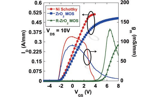
Figure 2: Transfer curves for Schottky-gated HEMT, ZrO2 MOS-HEMT, and recessed barrier ZrO2 MOS-HEMT.
The subthreshold swing (SS) was used to estimate interface trap densities (Dit). The lowest Dit was for the non-recessed MOS-HEMT. "This suggests that the ZrO2 gate oxide reduces the interface trap density at the AlGaN surface in the gate region," the researchers say.
The higher Dit of the recessed device was probably due to crystal damage from the recess etch process, according to the researchers. They add: "Current collapse was poor in this device structure, as the negative charge in the oxide will enhance the virtual gating effect rather than passivate it. An ideal device structure would implement PECVD SiNx in the access regions and ZrO2 under the gate; however, the process steps to enable this are still being developed."
The ZrO2 reduced gate leakage (IG) by four orders of magnitude.
http://doi.org/10.7567/APEX.9.071003
The author Mike Cooke is a freelance technology journalist who has worked in the semiconductor and advanced technology sectors since 1997.


