


- News
15 July 2016
Yellow-green indium gallium nitride quantum dot laser
Yellow-green lasing at 560.4nm wavelength has been achieved under continuous wave (CW) operation of indium gallium nitride (InGaN) quantum dot (QD) vertical-cavity surface-emitting laser (VCSEL) diodes at room temperature "for the first time", according to researchers based in China and Germany [Guoen Weng et al, Optics Express, vol24, p15547, 2016]. Previously, pulsed operation in the shorter-wavelength 503nm green region for VCSELs was achieved by Nichia.
Up to now, CW lasing in the 'green gap' has been elusive. InGaN-based devices suffer from strong charge polarization effects that can lead to large electric fields, particularly in strained layers resulting from lattice mismatching. These electric fields tend to pull electrons and holes apart, reducing recombination into photons. This is often referred to as the quantum-confined Stark effect (QCSE). QDs are one way to reduce strain effects that exacerbate the charge polarization effects in InGaN.
The high-indium-content InGaN needed for green emission tends to suffer from a severe drop in radiation efficiency. The team from China's Xiamen University, Suzhou Institute of Nano-tech and Nano-bionics, and East China Normal University, together with Technical University of Berlin in Germany, based their device on strong localization and negligible QCSE of QDs, as well as good coupling between the QD region and external electric fields. It was hoped that these factors would work together to give high radiation efficiency and thus lasing in the 'green gap'.
The device material was grown on (0001) sapphire using metal-organic chemical vapor deposition (MOCVD). The light-emitting active region consisted of two layers of InGaN QDs in a GaN barrier matrix. The GaN in the active region was grown in two temperature steps: 2nm at the 670°C used to make the QDs and 8nm at 850°C. The low-temperature GaN was used to protect the In0.27Ga0.73N from the subsequent ramp to 850°C. The dot density was around 1.5x10¹⁰/cm2, according to atomic force microscopy (AFM) scans. Electron microscope analysis gave dot diameters ranging between 20nm and 60nm with an average height of 2.5nm.
Device fabrication began with depositing and patterning silicon dioxide (SiO2) on the p-GaN surface of the grown material to create a 10μm diameter aperture, 30nm of indium tin oxide (ITO) as a p-contact and current-spreading layer, and chromium/gold around the aperture as electrode. A titanium dioxide (TiO2) phase shifter was added to put the ITO layer at a node of the radiation field and the active region at an anti-node. Further layers of SiO2 and TiO2 were used as a 12.5-pair distributed Bragg reflector (DBR) back mirror.
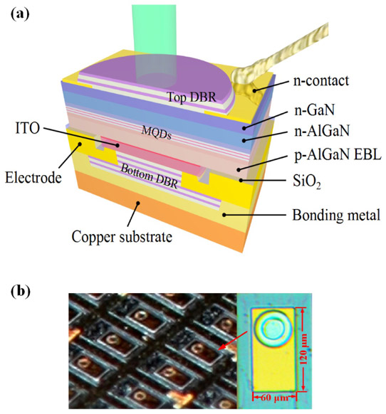
Figure 1: (a) Cross-sectional schematic of fabricated InGaN QD VCSEL. (b) Picture of array (left) and enlarged optical micrograph (right).
The device was then flipped and metal-bonded to a copper heat-sink before removal of the sapphire substrate through laser lift-off. The n-GaN layer was thinned using inductively coupled plasma (ICP) etch and chemical mechanical polishing (CMP). The 60μm x120μm VCSEL (Figure 1) was completed with an n-contact and 11.5-pair TiO2/SiO2 DBR.
Photoluminescence analysis of the device material on sapphire at room temperature gave a broad peak around 524nm wavelength with full-width at half maximum (FWHM) of the order of 50nm. The broadness of the peak was attributable probably to the large variation in QD size and composition. Low-temperature photoluminescence at 5K, with no identifiable blue-shift with excitation power increase on the long wavelength side, suggested that the QCSE was weak to negligible.
The threshold current and voltage were 0.61mA (0.78kA/cm2) and 6.7V, respectively. The researchers comment: "Such a low threshold is attributed to the high reflectivities of the DBR mirrors, the strong localization effect and the negligible QCSE in InGaN QDs, and a good coupling between QDs region and the electric field of the lasing mode". The team adds that filamentation effects due to "inhomogeneous distribution of refractive index caused by both indium content and the higher efficiency of carrier capture of QDs than the surrounding material" may also play a role.
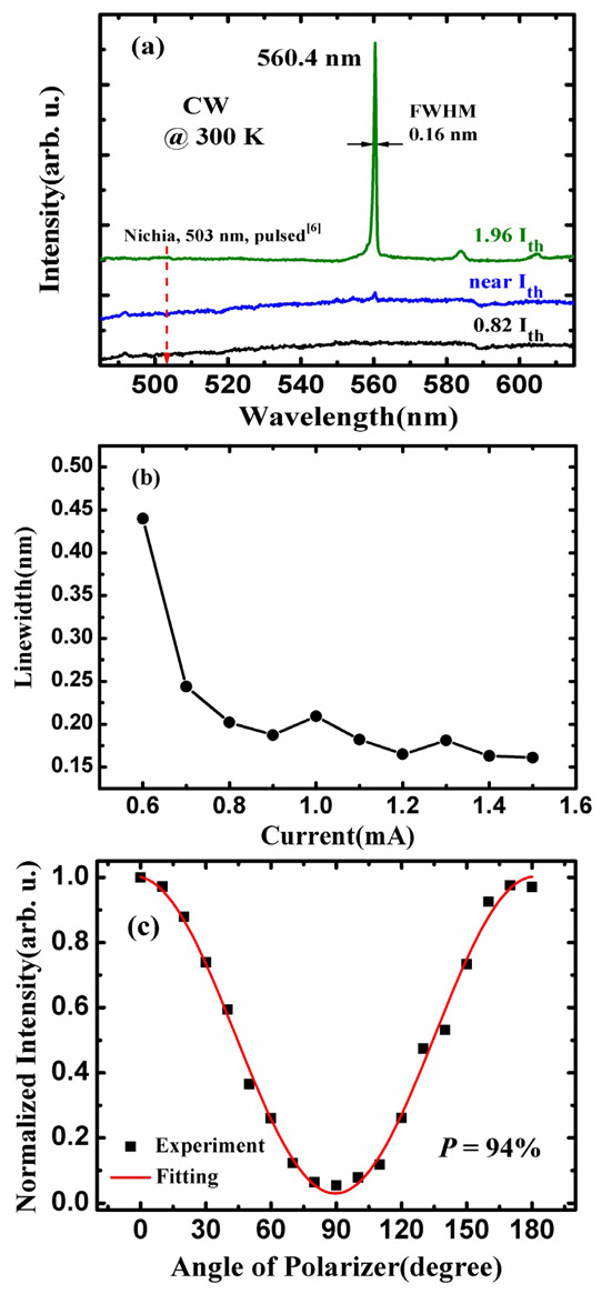
Figure 2: (a) Laser emission spectra at various injection current levels measured at 300K. (b) Laser emission linewidth versus injection current. (c) Polarization characteristics of laser emission at injection current of 1.96x threshold (Ith).
The measured full-width at half-maximum was 0.16nm, as limited by the setup resolution (Figure 2). The 24nm separation between lasing modes indicated a cavity length of 2.6μm. The polarization was 94% at 1.96x threshold current, a 30dB suppression of the orthogonal polarization.
Yellow-green InGaN quantum dot laser VCSEL InGaN MOCVD
http://dx.doi.org/10.1364/OE.24.015546
The author Mike Cooke is a freelance technology journalist who has worked in the semiconductor and advanced technology sectors since 1997.


