


- News
22 July 2016
LayTec adds nanoscale SPC for quaternary films to EpiNet 2016 analysis software
In its newsletters in April 2016 and June 2016 in-situ metrology system maker LayTec AG of Berlin, Germany reported on x-ray diffraction (XRD)-gauged nk database improvements for InGaAsP (indium gallium arsenide phosphide) and InGaAlAs (indium gallium aluminium arsenide) on indium phosphide (InP) and for ternary/quaternary materials on gallium arsenide (GaAs). The next release of LayTec's control and analysis software EpiNet 2016 (scheduled for fourth-quarter 2016) will offer completely new analysis features for customers interested in high-accuracy statistical process control (SPC) of related device growth processes.
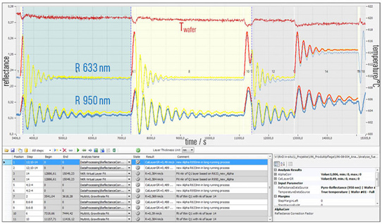
Picture: Screenshot of EpiNet 2016: data analysis of an InGaAsP/InP device structure on InP(001): the thickness of the three very thin InGaAsP layers in steps 2, 6, 10 is: 28.5nm, 48.7nm and 100.3nm, respectively. The table in the lower part of the figure gives the sequence of analysis functions for routine and automated SPC of this device growth process. T=temperature, R=reflectance.
The figure gives an example: the thickness of very thin InGaAsP layers in a device stack grown on InP(001) in an Aixtron Planetary Reactor is determined by a well selected set of automated analysis operations. First, several InP layers are utilized for permanent in-situ high-accuracy re-calibration of all reflectance channels (yellow lines) in long-lasting epi runs. Second, the lattice matching of the quaternary layers is verified by wafer bow analysis (not shown). Third, the composition of the quaternary material is determined at the thick InGaAsP layer in step #14. Finally, based on this information, the thicknesses of the thin InGaAsP layers in steps #2, #6 and #10 are accurately measured by double-wavelength thickness analysis.
For better understanding of growth processes, LayTec also offers related training courses for process engineers and quality managers.
LayTec's 21st in-situ seminar at ICMOVPE
At LayTec's 21st in-situ seminar on 11 July in conjunction with the 18th International Conference on Metal Organic Vapor Phase Epitaxy (ICMOVPE-XVIII) in San Diego, CA, USA, more than 80 researchers and engineers discussed the latest research results and learned about new in-situ metrology developments.
Dan Koleske of the USA's Sandia National Laboratories presented in-situ results of aluminium nitride (AlN)/sapphire growth measured by an EpiCurveTT tool on his Taiyo Nippon Sanso SR4000 MOCVD reactor.
Gary Tompa of Structured Materials Industries Inc (SMI) of Piscataway, NJ, USA focused on the integration and utilization of an EpiTT tool in SMI's Ga2O3 MOCVD system.
Hilde Hardtdegen of Research Center Juelich in Germany reported on finding narrow growth temperature windows for novel Ge1Sb2Te4 2D materials by combining reflectance and temperature sensing of an EpiR TT tool on her Aixtron AIX 200 MOCVD reactor.
Finally, LayTec's Oliver Schulz gave an overview of the latest modular adaptations of the new Gen3 product lines to AIX CRIUS, AIX 6x2" and Veeco K700 MOCVD reactors.
Following tradition, the second half of the seminar was devoted to in-depth discussions with and between customers.
In-situ lattice-match sensing with XRD resolution by EpiCurveTT Gen3
At ICMOVPE XVIII, LayTec presented the talk 'MOCVD of InGaAsP/InP-based device structures: full replacement of ex-situ process calibration by advanced in-situ metrology'. The work is a result of a collaboration between the team of Tony SpringThorpe at the National Research Council (NRC) of Canada, Christoph Hums and co-workers at Fraunhofer HHI (Heinrich Hertz Institute) in Berlin, Germany, and LayTec.
During lattice-matched growth of InGaAs on InP in an Aixtron CRIUS reactor, the high-resolution wafer bow sensing (EpiCurveTT Gen3 with ARS module) reached a resolution of 0.2km-1. Two effects that contribute to the wafer bow were carefully separated: the lattice mismatch between layer and substrate and the vertical temperature gradient across the wafer resulting from temperature difference between the wafer pocket and showerhead.
As a result, the lattice match of InGaAs to InP could be tuned in-situ with ±50ppm resolution – an accuracy that formerly could be achieved only by ex-situ x-ray diffraction (XRD), notes LayTec.
Aixtron qualifies LayTec EpiNet 2016 software
Accuracy of LayTec EpiTT Gen3's XRD-referenced nk database improved for InP-based materials
LayTec issues improved n.k database for III-nitrides in EpiNet 2015 release
LayTec Metrology MOCVD Aixtron EpiCurveTT EpiTT HHI


