


- News
19 January 2016
Increasing gallium nitride MOSFET threshold voltage
University of Electronic Science and Technology of China claims a record high threshold voltage of +7.6V for an aluminium oxide/gallium nitride (Al2O3/GaN) metal-oxide-semiconductor field-effect transistor (MOSFET) [Qi Zhou et al, IEEE Electron Device Letters, published online 22 December 2015]
GaN transistors tend to be normally-on with negative threshold voltages without special measures designed to increase the threshold for normally-off operation. These measures tend to negatively impact other factors such as reducing on-current and/or increasing off-current/leakage.
Normally-off operation is particularly desired for power applications where fail-safety and power efficiency are important considerations. In particular, a threshold above 6V and a gate swing greater than 10V are often needed to avoid faulty turn-on induced by electromagnetic interference in power switching applications.
MOSFETs tend to have more positive thresholds compared with Schottky gate high-electron-mobility transistors (HEMTs). However, the dielectric/semiconductor interface in a MOSFET can create a positive fixed charge in trap states, impeding normally-off operation. Fixed charges can also act as scattering centers that reduce the field-effect mobility, increasing on-resistance.
 2O3/GaN MOSFETs and (b) surface morphology of recessed gate region." width="542" height="189" />
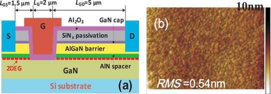
Figure 1: (a) Schematic cross section of normally-off Al2O3/GaN MOSFETs and (b) surface morphology of recessed gate region.
The researchers fabricated their MOSFETs (Figure 1) on a commercial 4-inch AlGaN/GaN-on-silicon wafer from Enkris Semiconductor (www.enkris.com). The metal-organic chemical vapor deposition (MOCVD) heterostructure consisted of a 3.5μm GaN buffer, 1nm AlN spacer, 23nm AlGaN barrier, and 2nm GaN cap. The specifications of the two-dimensional electron gas (2DEG) were 1.05x10¹³/cm2 carrier density, 1500cm2/V-s mobility, and 400Ω/square sheet resistance.
The ohmic contacts were fabricated before mesa isolation etching. The 100nm silicon nitride (SiNx) passivation was applied using inductively coupled plasma chemical vapor deposition (ICP-CVD).
The SiNx was also used as a hard mask for a two-step gate recess etching with inductively coupled plasma and a low-damage digital process. The 5Å digital etch cycle consisted of oxygen plasma oxidation and dilute hydochloric acid rinse for oxide removal.
Using 15 cycles of the digital etch resulted in a recess depth of about 30nm into the heterostructure, around 4nm over-etch into the buffer/2DEG layer. The recess root mean square (RMS) surface roughness was 0.54nm, according to atomic force microscopy.
The gate stack consisted of 18nm of atomic layer deposition (ALD) aluminium oxide (Al2O3) and nickel/gold. Annealing at 400°C in nitrogen was applied either post-dielectric (PDA) or post-gate (PGA) deposition.
The threshold voltage for 1μA/mm current (VTH') at 10V drain bias was -1.9V without annealing. This normally-on behavior was shifted to normally-off +2.7V with PGA. PDA devices had an even higher threshold of +5.2V.
Capacitance-voltage measurements were consistent with Al2O3/GaN interface trap densities of 1.44x10¹³/cm2, 5x10¹²/cm2, and 3x10¹²/cm2 for no annealing, PGA, and PDA, respectively.
The researchers believe that the interface traps result in positive charges that shift the threshold downwards: "The presence of interface positive charges can be explained by two possible scenarios. 1) The GaN surface is metal (Ga)-face, the oxygen atoms of Al2O3 attach to Ga substituting for N (ON) and forming Ga-O bond at Al2O3/GaN interface due to the low formation energy of ON. The ON is likely to act as a shallow donor in GaN and positively charged (ON+). 2) The Ga dangling bonds (DBs) could be generated during gate recessing and act as the positive charge centers."
The team suggests that the nitrogen from the annealing more easily reaches the interface if applied post-dielectric rather than post-gate. This nitrogen fixes the ON and DB problems.
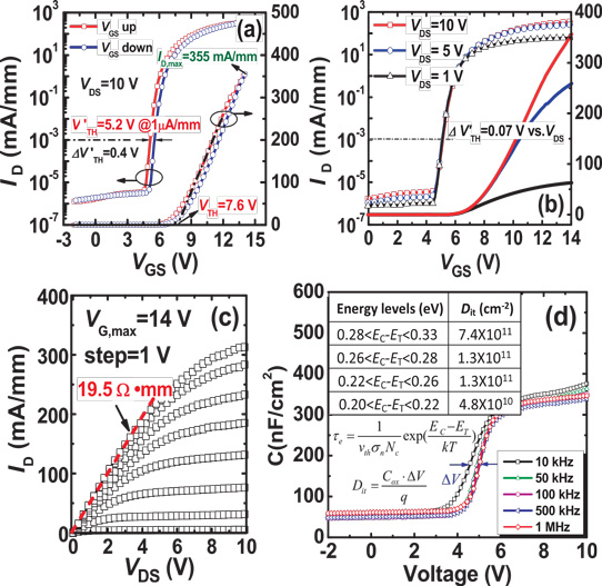
Figure 2: (a) Measured transfer curves in linear- and log-scale, (b) transfer curves versus drain bias (VDS), (c) output curves and (d) frequency-dependent capacitance-voltage (C-V) curves of PDA device. Inset: extracted interface state energy levels and corresponding state density (Dit). Sweep rate 0.25V/s.
A PDA device with 2μm gate length demonstrated a threshold voltage (VTH) for the linear region of +7.6V (Figure 2). The gate-source and gate-drain distances and gate width were, respectively, 1.5μm, 5μm, and 50μm. The gate had an overhang of 0.5μm on either side. The maximum drain current of 355mA/mm was achieved at +14V gate potential.
The researchers comment: "These values are the highest reported for normally-off GaN devices with VTH > 5V up to date. The device features an excellent pinch-off at VGS of ∼ +4.6V, and delivers a low off-state leakage current of 1.8nA/mm at VGS = 0V. The VTH also exhibits good stability versus drain bias voltage."
The researchers also point out that the +5.2V value for the more stringent VTH' criterion is remarkable. Other groups with normally-off devices have reported only up to +2.7V for this VTH' criterion, according to a comparison table assembled by the team. The same table gives a maximum VTH of +7.2V for the other groups.
http://ieeexplore.ieee.org/xpl/login.jsp?tp=&arnumber=7361977
The author Mike Cooke is a freelance technology journalist who has worked in the semiconductor and advanced technology sectors since 1997.


