


- News
25 January 2016
Aluminium ion implants for lateral gallium nitride transistors
Researchers in China have been studying the potential of aluminium (Al) ion implantation for creating back-barriers and device isolation in gallium nitride (GaN) metal-insulator-semiconductor high-electron-mobility transistors (MISHEMTs) on silicon substrates [Shichuang Sun et al, Appl. Phys. Lett., vol108, p013507, 2016].
The team from Huazhong University of Science and Technology and Suzhou Institute of Nano-Tech and Nano-Bionics (SINANO) comments that, with optimization, Al ion implantation offers a great potential method for creating high-performance AlGaN/GaN HEMTs.
The resulting devices showed much reduced off-current with only a small impact on the on-current. GaN transistors are being developed for high-voltage switching and high-frequency power amplification.
The 600nm resistive GaN buffer was grown on (111) silicon with an AlGaN/AlN transition layer by metal-organic chemical vapor deposition (MOCVD). The aluminium implant was carried out at two energies (140keV/90keV) to give a uniform ion profile.
The templates were cleaned and thermally treated before MOCVD regrowth. The thermal process consisted of a 12 minute ramp up to 1050°C in ammonia/hydrogen and then maintaining the temperature for a further 5 minutes. The treatment aimed to repair lattice damage from the ion implant. The thermal process was carried out in the MOCVD chamber.
The re-growth sequence was 100nm undoped GaN, a 1nm AlN interlayer, a 20nm Al0.25Ga0.75N barrier, and a 3nm GaN cap. The researchers claim that there was no observable damage at the interface with the ion-implanted template.
The Hall resistance and carrier concentration in the two-dimensional electron gas (2DEG) channel region were 350Ω/square and 1.07x10¹³/cm2, respectively. A wafer subjected to the same process apart from the ion implant had 315Ω/square resistance and 1.3x10¹³/cm2 carrier concentration.
The transistor fabrication began with low-pressure CVD of 20nm silicon nitride for gate insulation. Annealed source/drain contacts consisted of titanium/aluminium/nickel/gold. Device isolation was achieved through more ion implantation. The gate electrode consisted of nickel/gold. The gate was 4μm long and 100μm wide. The distances from gate to drain and source were 16μm and 4μm, respectively.
The device built on the sample without ion implantation (A) did not achieve pinch-off and the on/off current ratio was very low at 46 (Figure 1). The ion-implanted device (B) was much better with "excellent pinch-off", according to the researchers. The on/off current ratio was 2.5x10⁵ with an off-current of 2.8x10⁻³mA/mm.
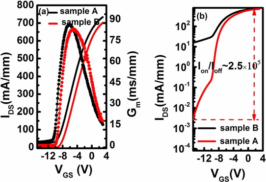
Figure 1: Transfer characteristics of AlGaN/GaN MISHEMTs on sample A and B templates.
The maximum drain current at 3V gate potential was 701mA/mm. The peak transconductance was 83mS/mm. The researchers say that there was little degradation in these parameters, compared with sample A.
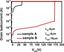 Figure 2: Measured breakdown voltage of AlGaN/GaN MISHEMTs on sample A and B templates.
The improvement in switching capability of sample B came from the much reduced off-current (Figure 2). The off-current was reduced by three orders of magnitude and the breakdown voltage increased by 5x, compared with sample A.
AlGaN back-barriers have also been used to improve off-currents. However, the 2DEG carrier concentration tends to be impacted more severely due to the charge polarization contrast of the AlGaN and GaN chemical bonds. Typical AlGaN back-barriers use around 5% Al content, giving a conduction-band offset of 0.06eV. The researchers estimate that the offset from the Al implantation is 0.07eV, equivalent to an Al0.058Ga0.942N layer.
Al ion implantation GaN MISHEMTs AlGaN/GaN HEMTs Silicon substrates MOCVD
http://dx.doi.org/10.1063/1.4939508
The author Mike Cooke is a freelance technology journalist who has worked in the semiconductor and advanced technology sectors since 1997.


