


- News
27 January 2016
Indium gallium arsenide on insulator n-channel fin field-effect transistors
IBM Research GmbH in Switzerland has developed an n-channel indium gallium arsenide (InGaAs) on insulator fin field-effect transistor (finFET) process and claims the highest on-current to date for CMOS-compatible InGaAs devices integrated on silicon (Si) [Vladimir Djara et al, IEEE Electron Device Letters, published online 1 January 2016].
The InGaAs-OI/Si wafer was produced using metal-organic chemical vapor deposition (MOCVD) and direct wafer bonding. The 20nm In0.53Ga0.47As layer was doped with ~5x10¹⁷/cm3 silicon. The buried oxide (BOX) insulator layer was 37nm thick.
Transistor fabrication (Figure 1) began with a digital wet etch of fins 15nm wide and 17nm high. A dummy gate was formed before creating 12nm silicon nitride (SiNx) spacers with plasma-enhanced atomic layer deposition (PEALD) and dry etching.
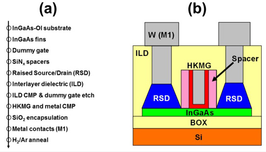
Figure 1: (a) CMOS-compatible RMG fabrication process flow and (b) cross-section schematic of the self-aligned InGaAs-OI FinFET architecture.
The raised source-drain (RSD) In0.53Ga0.47As contacts were re-grown using selective low-temperature MOCVD. The contacts were doped with ~6x10¹⁹/cm3 tin.
A 250nm interlayer dielectric was applied by plasma-enhanced chemical vapor deposition (PECVD). The material was subjected to chemical mechanical polishing (CMP) that exposed the dummy gate; the dummy gate was then removed.
PEALD was used to create a high-k aluminium oxide/hafnium dioxide metal gate stack (HKMG) with a capacitance equivalent thickness of ~1.5nm. The gate metal was 150nm tungsten. This tungsten layer was planarized with CMP.
The device was encapsulated in silicon dioxide and metal contact pads created. An optimized hydrogen/argon anneal was carried out to reduce the interface trap density to ~1.5x10¹²/cm2-eV at 0.25eV below the conduction band edge, according to high-low frequency capacitance-voltage analysis.
The gate leakage current for a 50nm gate-length (LG) transistor was below 400pA/μm with 0.5V and gate potential in the range -0.2V to +1V. The saturation transconductance peaked at ~615μS/μm. The saturation subthreshold swing had a minimum of 92mV/decade. The drain-induced barrier lowering (DIBL) was 57mV/V. The threshold in saturation was 0.09V.
The on-current (ION) was 156μA/μm (Figure 2). The researchers comment: "Although the ION value of 156μA/μm obtained at LG = 50nm represents the highest value reported to date for CMOS-compatible InGaAs FETs integrated on a Si platform, significant improvements are still needed to reach the performance of state-of-the-art III-V n-FETs integrated on bulk InP and be competitive for advanced technology nodes. We speculate that the required performance boost could be obtained through the use of source and drain extensions."
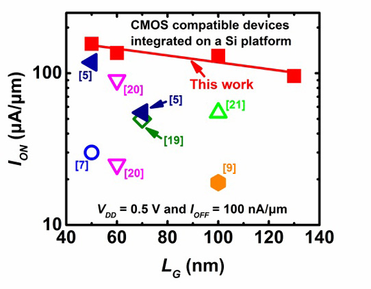
Figure 2: ION vs LG benchmark of CMOS-compatible InGaAs FETs integrated on Si platform. ION values are extracted at 0.5V operating voltage and IOFF of 100nA/μm.
Long 1μm-gate devices had a 106 maximum/minimum drain current ratio and subthreshold swing of 62mV/decade.
InGaAs on insulator finFET InGaAs finFET MOCVD PECVD
http://ieeexplore.ieee.org/xpl/articleDetails.jsp?arnumber=7370755
The author Mike Cooke is a freelance technology journalist who has worked in the semiconductor and advanced technology sectors since 1997.


