


- News
13 January 2016
Vertical p-n diodes on bulk gallium nitride result in avalanche
Researchers in USA and Japan continue to report on recent developments of vertical p-n diode produced on bulk gallium nitride (GaN) [Kazuki Nomoto et al, IEEE Electron Device Letters, published online 8 December 2015]. The team consisted of personnel from Cornell University and University of Notre Dame in the USA and Quantum Spread Ltd and Hosei University in Japan.
The researchers comment: "The textbook-like behavior in our GaN p-n power diodes, with avalanche capability demonstrated in this work, signifies the quality of epitaxial GaN is now on par with that of SiC [silicon carbide] while the performance and yield of large-area power devices will most likely improve dramatically with further reduction of threading dislocations in bulk GaN substrates."
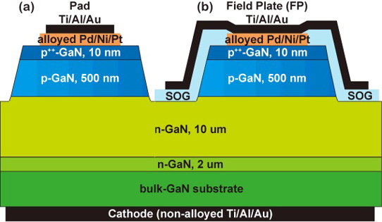
Figure 1: Schematic cross-sections of the GaN-on-GaN p–n junction diodes (a) without (w/o) field-plate (FP) and (b) with FP.
The work was in part supported by the US Advanced Research Projects Agency-Energy (ARPA-E) Strategies for Wide Bandgap, Inexpensive Transistors for Controlling High-Efficiency Systems (SWITCHES) Program. Cornell, Notre Dame et al have published a number of papers and conference presentations in the past month [Some of which have been reported here: www.semiconductor-today.com/news_items/2015/dec/und_291215.shtml; www.semiconductor-today.com/news_items/2015/dec/cornell_241215.shtml; www.semiconductor-today.com/news_items/2015/dec/iqe-notredame-cornell_231215.shtml].
The vertical diode material was grown on bulk 2-inch-diameter 400μm-thick GaN using metal-organic vapor phase epitaxy (also known as metal-organic chemical vapor deposition). The n-GaN buffer and drift layers had 2x10¹⁸/cm3 and 1-2x10¹⁶/cm3 silicon doping, respectively. The researchers took particular care to restrict carbon and oxygen impurities in the drift layer to 1.2x10¹⁶/cm3 and 1.7x10¹⁶/cm3, respectively. The p-GaN and p++-GaN layers had respective magnesium concentrations of 1x10¹⁸/cm3 and 2x10²⁰/cm3. The doping and impurity levels were determined from secondary-ion mass spectrometry on calibration wafers.
Cathodoluminescence indicated threading dislocation densities of ~106/cm2 in the epitaxial layers, comparable to the level in the underlying bulk GaN. The researchers comment that this level is two orders of magnitude lower than for heteroepitaxial material on non-GaN substrates such as SiC.
After growth, the epitaxial material was annealed at 700°C to activate the magnesium doping. The hole concentration in the p-GaN was 7.4x10¹⁶/cm3 with 27cm2/V-s mobility, according to Hall measurements at 25°C.
Diodes with and without a field-plate (FP) were fabricated. The FP extended over the whole circular diode mesa. Spin-on-glass (SOG) insulation (200nm thick) was used to reduce reverse leakage currents. The anode consisted of palladium/nickel/platinum (Pd/Ni/Pt), deposited before the SOG. The curing of the SOG at 425°C for 30 minutes also affected the composition of the anode metals to give some alloying effect. The cathode on the substrate back-side consisted of titanium/aluminium/gold (Ti/Al/Au). This metal composition was also used for the FPs.
The researchers say that they used the best of at least three devices to indicate the potential of GaN-on-GaN technology. Diode sizes were based on the bottom of the mesa diameter. The substrate was not thinned. Thinning would reduce series resistance effects.
The diode's ideality factor between 2V and 2.5V forward bias was ~2.0, indicative of Shockley-Read-Hall (SRH) recombination through trap states in the middle of the bandgap. Above 2.5V, the ideality trends downwards to ~1.3 near 2.8V, indicating a decrease of recombination and increase of diffusion current across the depletion region. The SRH lifetime was estimated at 12ns. The turn-on voltage was around 3.0V, close to the 3.4eV GaN bandgap. The current below 2V forward bias was too low to be measured. The current swing was more than 14 orders of magnitude.
The differential specific on-resistance (Ron) of a 107μm diameter diode was ~0.4mΩ-cm2 at ~3kA/cm2, or 0.55mΩ-cm2, including a factor for current spreading that effectively increases the diameter to 127μm. In fact, these values were lower than a theoretical estimate of 0.64mΩ-cm2. "The difference may be attributed to the underestimated electron mobility or conduction modulation in p-n diodes, demanding further studies," the researchers comment.
The breakdown (BV) for 107μm-diameter diodes under reverse bias was around 830V without FPs and around 1706V with FPs. The diode without FP failed near the mesa edge. An increase in leakage current above 500V with FPs was attributed, most likely, to a leakage path introduced by the FP fabrication process. The BV2/Ron Baliga figure of merit with FP was 5.3GW/cm2 ((1706V)2/0.55mΩ-cm2).
The BV was nearly independent of diode diameter for devices without FP. However, with FPs the BV decreases with increasing diameter (~1.2kV with 707μm diameter). At the same time, the Ron value increased with diameter (Figure 2).
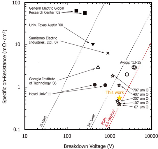
Figure 2: Benchmark plot of BV versus Ron in reported GaN p-n diodes. The solid star is the result obtained in diodes with an effective diode diameter of 127μm taking into account effect of current spreading. Hollow stars are results using diode mesa bottom-diameter. Dotted lines are unipolar limit, where mobility of 1100cm2/Vs and critical field of 3.4MV/cm are used for GaN (8.5GW/cm2).
Based on the drift region thickness of 10μm, the researchers estimate a critical field of more than 3.5MV/cm. This is based on an ideal planar model and assuming 75% of the resultant maximum breakdown to allow for the non-ideal nature of the diode. The estimated critical field is among the best reported, according to the researchers.
The breakdown voltage increased with temperature to 1778V at 125°C – a signature of avalanche breakdown, according to the researchers. The temperature of the 1706V BV was 25°C.
Vertical p-n diodes Bulk GaN GaN MOVPE MOCVD
http://ieeexplore.ieee.org/xpl/login.jsp?tp=&arnumber=7349157
The author Mike Cooke is a freelance technology journalist who has worked in the semiconductor and advanced technology sectors since 1997.


