


- News
17 February 2016
Triangular nanostructure semi-polar gallium nitride light-emitting diodes
University of New Mexico (UNM) in the USA has fabricated triangular-nanostripe core–shell semi-polar III–nitride light-emitting diodes (TLEDs, Figure 1) on c-plane sapphire [Ashwin K. Rishinaramangalam et al, Appl. Phys. Express, vol9, p032101, 2016]. The performance results are described as "preliminary".
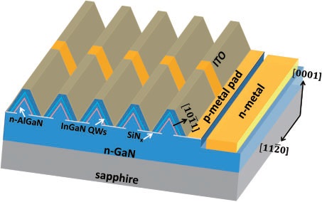
Figure 1: Illustration of section of triangular-stripe core–shell nanostructure LED.
The researchers comment: "Upon optimization of these TLEDs to being on par with existing technologies on free-standing GaN, the low cost associated with this approach could potentially become the driving force towards commercial adoption."
Semi-polar and non-polar LEDs should have improved performance due to reduced electric fields arising from charge polarization discontinuities of the III-nitride chemical bonds at heterointerfaces. The electric fields pull the electrons and holes apart, reducing recombination into photons. However, semi-polar/non-polar structures are generally grown on small, very expensive free-standing gallium nitride (GaN) substrates.
By using triangular nanostripes with semi-polar sidewalls, the UNM researchers hope to access the advantages for light-emission without the non-commercial costs of free-standing substrates.
The researchers prepared a 2μm n-GaN on sapphire template using metal-organic chemical vapor deposition (MOCVD). A 120nm silicon nitride layer was patterned into micron-scale stripes using interferometric lithography. The silicon nitride dielectric also functioned as electrical insulation in the resulting devices. A second lithography step was used to define the device and contact regions. The exposed regions of the silicon nitride were dry etched and the wafer surface cleaned using a 'piranha solution' process before nanostructure growth.
The new growth was carried out with continuous-flow MOCVD. The core was silicon-doped n-GaN. The fast growth of the c-plane leads to the emergence of a triangular cross-section with semi-polar (10-11)-plane sides.
The researchers then applied a thin n-type aluminium gallium nitride (AlGaN) layer to block reverse leakage currents, to getter oxygen impurities, and to fill defects in the silicon nitride mask/insulation.
Further growth consisted of n-GaN electron injection, four indium gallium nitride (InGaN) quantum wells (QWs) in GaN barriers (3nm/9nm), and finally a p-GaN contact. The c-plane surfaces on the apex of the triangular cross-section re-emerged during p-GaN growth. The researchers attribute this to the use of hydrogen-rich growth conditions and the faster growth (~3x) of p-GaN on the (10-11) plane, compared with the c-plane.
LEDs were fabricated with an indium tin oxide (ITO) transparent conducting current-spreading layer, titanium/aluminium/nickel/gold n-electrode, and titanium/gold n- and p-contact pads.
The devices were tested under pulsed currents (2μsecond, 2% duty cycle). The emission was broadband and a significant wavelength blue-shift was seen with increasing current (Figure 2). Wavelength shifts with semi-polar devices are usually much smaller than those of c-plane LEDs. Since the peak was to one side of the broadband of emitted radiation, the researchers used the dominant wavelength to characterize the shift. At 50A/cm2 current density, the dominant wavelength was ~465nm compared with a peak at ~425nm.
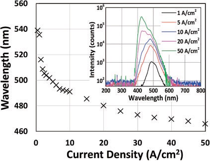
Figure 2: Electroluminescence dominant wavelength as a function of current density. Inset: electroluminescence spectra.
Electron microscope analysis showed the quantum well thicknesses to be non-uniform, thus explaining the broadband emission. The wells were thicker near the apex of the triangular cross-section. The researchers also believe that long-range variation in indium composition of the quantum wells played a role in the broadband nature of the spectra. Energy-dispersive x-ray spectroscopy revealed an indium composition 1.5x higher nearer the apex compared with the sidewall.
The researchers explain: "For low injection currents, the path of least resistance is through the thick, high-indium-content QWs near the apex. This results in longer-wavelength emission (∼480nm) at low current density, primarily from the QWs near the apexes. As the current density is increased, the current spreading across the nanostructure is improved and a short-wavelength EL peak near 425nm emerges. This peak is attributed to the thin, low-indium-content QWs on the main sidewalls of the triangular stripe. The peak near 425nm shows very small shift in wavelength as a function of current density, as expected for uniform semi-polar QWs."
TLEDs GaN c-plane sapphire MOCVD
http://doi.org/10.7567/APEX.9.032101
The author Mike Cooke is a freelance technology journalist who has worked in the semiconductor and advanced technology sectors since 1997.


