


- News
11 February 2016
TU Munich grows pulsed IR-emitting GaAs nanowire lasers on silicon chip
The Technical University of Munich (TUM) has developed III-V semiconductor nanowire lasers grown directly on a silicon chip, making it possible to produce high-performance photonic components cost-effectively, it is reckoned, and paving the way in future for fast and efficient data processing with light.
The miniaturization of electronics is now reaching its physical limits, says TUM. "Today already, transistors are merely a few nanometers in size. Further reductions are horrendously expensive," notes professor Jonathan Finley, director of the Walter Schottky Institute at TUM. "Improving performance is achievable only by replacing electrons with photons," he adds.
Data transmission and processing with light has the potential of breaking the barriers of current electronics. Silicon-based photonics chips already exist, but the sources of light for transmitting data must be attached to the silicon in complicated and elaborate manufacturing processes.
Instead, Dr Gregor Koblmüller of TUM's Department of Semiconductor Quantum-Nanosystems has, in collaboration with Jonathan Finley, developed a process to deposit nanolasers directly onto silicon chips. A patent for the technology is pending.
"The two materials [III-V and silicon] have different lattice parameters and different coefficients of thermal expansion. This leads to strain," notes Koblmüller. "For example, conventional planar growth of gallium arsenide onto a silicon surface results therefore in a large number of defects."
Instead, by depositing nanowires that are free-standing on silicon, their footprints are merely a few square nanometers. The TUM team could hence preclude the emergence of defects in the GaAs material.
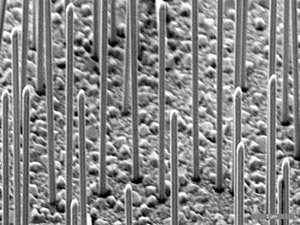 Picture: Nanowires on a silicon surface.
To generate coherent light, photons must be reflected at the top and bottom ends of the nanowire (forming a vertical-cavity laser), amplifying the light until it reaches the desired threshold for lasing.
To fulfil these conditions, the researchers needed to develop a simple yet sophisticated solution: "The interface between gallium arsenide and silicon does not reflect light sufficiently," says Benedikt Mayer, doctoral candidate in the team led by Koblmüller and Finley. "We thus built in an additional mirror – a 200nm-thick silicon oxide layer that we evaporated onto the silicon," he adds. "Tiny holes can then be etched into the mirror layer. Using epitaxy, the semiconductor nanowires can then be grown atom for atom out of these holes."
Only after the wires protrude beyond the mirror surface can they grow laterally – until the semiconductor is thick enough to allow photons to pass back and forth to allow stimulated emission and lasing. "This process is a very elegant because it allows us to position the nanowire lasers directly also onto waveguides in the silicon chip," says Koblmüller.
Currently, the new GaAs nanowire lasers produce infrared light at a predefined wavelength and under pulsed excitation. "In the future we want to modify the emission wavelength and other laser parameters to better control temperature stability and light propagation under continuous excitation within the silicon chips," says Finley. The team has just published its first successes in this direction ('Monolithically Integrated High-beta Nanowire Lasers on Silicon', B. Mayer et al, Nano Lett. (2016) 16 (1), p152, http://pubs.acs.org/doi/full/10.1021/acs.nanolett.5b03404; 'Coaxial GaAs-AlGaAs core-multishell nanowire lasers with epitaxial Gain control', T. Stettner et al, Appl. Phys. Lett. (2016) 108, 011108, http://dx.doi.org/10.1063/1.4939549; 'Continuous wave lasing from individual GaAs-AlGaAs core-shell nanowires', B. Mayer et al, Appl. Phys. Lett. (2016) 108, vol. 8, to appear on 22 Feb).
The team now targets another goal. "We want to create an electric interface so that we can operate the nanowires under electrical injection instead of relying on external lasers," says Koblmüller.
"The work is an important prerequisite for the development of high-performance optical components in future computers," concludes Finley. "We were able to demonstrate that manufacturing silicon chips with integrated nanowire lasers is possible."
The research was funded by the German Research Foundation (DFG) through the TUM Institute for Advanced Study, the Excellence Cluster Nanosystems Initiative Munich (NIM) and the International Graduate School of Science and Engineering (IGSSE) of the TUM, as well as by IBM through an international postgraduate program.
Nanolasers GaAs nanowires III-Vs-on-Si


