


- News
12 February 2016
TSMC researchers claim first indium arsenide fin field-effect transistor
Researchers led by TSMC R&D Europe B.V. in Belgium claim the first demonstration of an unstrained indium arsenide (InAs) fin field-effect transistor (finFET) with 20nm fin height (Hfin) [R. Oxland et al, IEEE Electron Device Letters, published online 29 January 2016]. The team also included researchers from University of Glasgow in the UK, Texas State University in the USA, and TSMC in Taiwan.
The use of InAs rather than indium gallium arsenide (InGaAs) should increase mobility, lowering on-resistance. The finFET configuration should give better electrostatic control over channel conduction compared with planar devices. Since the present devices were the first of their kind, they did well to give performance comparable in some respects with scaled and optimized planar transistors.
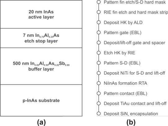
Figure 1: (a) Layer structure used, showing the pseudomorphic InAlAs etch-stop layer and (b) process flow for fabrication of InAs finFETs, starting with first step after wafer growth.
The finFET material was grown by molecular beam epitaxy (MBE) on p-InAs substrates (Figure 1). The 500nm undoped lattice-matched buffer was designed to isolate the 20nm undoped InAs channel from the conducting substrate. A quaternary indium aluminium arsenide antimonide (InAlAsSb) buffer composition gives improved top interface flatness, process and composition repeatability, and increased oxidation resistance over ternary AlAsSb, according to the researchers. Further carrier confinement was provided by the pseudomorphically strained 7nm InAlAs layer between the InAs channel and InAlAsSb buffer.
The fins were etched using inductively coupled plasma (ICP) etch with methane, hydrogen, chlorine and oxygen chemistry. The fin height was 20nm and the width (Wfin) was 25-35nm. The InAlAs acts as an etch stop, protecting the structure from uncontrolled oxidation, which is a particular concern for etching compound Sb-based semiconductors containing aluminium.
Before forming the gate stack, native oxide was removed before controlled oxygen termination. The gate insulation consisted of 5nm of atomic layer deposition (ALD) zirconium dioxide, giving 1.2nm equivalent oxide thickness (EOT). The gate metal was palladium. Spacers consisted of silicon nitride. The gate length (Lg) was 1μm.
The devices consisted of 10 fins. The 3μm-wide source/drain electrodes were fabricated from nickel/titanium, which was annealed to give a NiInAs metallic phase. Titanium and gold were then applied for contacts. The devices were encapsulated in 50nm of silicon nitride. The encapsulation also induced electrostatic source/drain extensions by pinning the Fermi level inside the conduction band of the InAs quantum well.
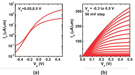
Figure 2: (a) Drain current versus gate voltage (Id-Vg) of typical device at 0.5V and 0.05V drain bias (Vd). (b) Drain current and voltage of same device with Vg = -0.25V to 0.50V in steps of 50mV.
A 25nm-wide fin device had a minimum subthreshold swing (S) of 148mV/decade with 0.5V drain bias. The extrinsic transconductance (gm) was 650μA/μm. The minimum drain current was 110nA/μm with -0.5V gate potential. Gate leakage was less than 2x10⁻⁸A/μm for the entire measurement range. The drain-induced barrier lowering (DIBL) was 27mV/V – this compares well with the 30mV/V value of a planar InAs device of similar gate length.
A device with wider 35nm fins had 310mV/decade subthreshold swing and 1430μS/μm extrinsic transconductance with 0.5V drain. The minimum drain current of 8μA/μm occurred at -0.5V gate potential. The gate leakage was the same as for the 25nm devices. The higher off-state current was attributed to reduced gate control from the wider fin and the different interface trap densities on the sidewall and top surface.
The Q-factors gm/S for the 25nm-wide and 35nm-wide finFETs were 4.4 and 4.8, respectively. The researchers compared their devices to the InGaAs finFETs of other groups (Table 1).
Table 1: Benchmark of III-V finFET devices. Quoted gm and S values extracted at Vd = 0.5V on same device where given, otherwise not reported. Bold entry (top) is TSMC finFET. Italic entry is planar device, included for comparison. InAs channel quantum well thickness is 10nm.
| InAs mole fraction | Hfin (nm) | Wfin (nm) | Lg (nm) | gm (μS/μm) | S (mV/dec) |
| 1.0 | 20 | 25 35 |
1000 1000 |
650 1430 |
148 310 |
| 0.7 | 25 | 50 | 100 | 280 | 190 |
| 0.53 | 40 | 40 | 60 | 1100 | 95 |
| 0.53 | 20 | 30 | 80 | 1800 | 82 |
| 0.7 | 10 | 20 | 120 | 1620 | 114 |
| 0.53 | 16 | 40 | 200 | - | 150 |
| 0.53a | 9 | 40 | 30 | 1640 | 84 |
| 1.0 | - | - | 130 | 2720 | 85 |
a. Mole fraction averaged over total fin height, including InAs quantum well (3nm) and In0.3Ga0.7As cladding layers (6nm in total).
http://ieeexplore.ieee.org/xpl/articleDetails.jsp?arnumber=7395313
The author Mike Cooke is a freelance technology journalist who has worked in the semiconductor and advanced technology sectors since 1997.


