


- News
24 February 2016
HRL creates low-carbon gallium nitride layers for Schottky barrier diodes
HRL Laboratories LLC in the USA has been developing vertical gallium nitride (GaN) Schottky barrier diodes (SBDs) with low turn-on voltages of 0.77V and breakdown at more than 800V [Y. Cao et al, Appl. Phys. Lett., vol108, p062103, 2016].
Vertical GaN structures have recently been studied with a view to high-voltage/power/frequency electronics, based on the material's high critical field for breakdown. Vertical current flow can push the peak field into the material, avoiding premature breakdown through surface states and passivation effects. A number of groups have reported on vertical p-n diodes on free-standing and bulk GaN, but these have high turn-on voltages around 3V. SBDs should have much lower turn-on voltages, reducing conduction losses during operation.
The researchers first studied the effect of different metal-organic chemical vapor deposition (MOCVD) growth conditions on carbon incorporation by creating a stack of GaN layers separated by AlGaN spacers on free-standing GaN. The carbon concentration varied between less than 3x10¹⁵/cm3 and 3x10¹⁹/cm3 (Table 1).
Table 1: Growth conditions for different carbon concentrations. Temperature around 1040°C for all layers.
| Layer | Pressure (Torr) | V/III ratio | Growth rate (Å/s) | Carbon (/cm3) |
| A | 50 | 954 | 6.99 | 3x10¹⁹ |
| B | 100 | 1717 | 7.14 | 8x10¹⁷ |
| C | 100 | 3981 | 3.76 | 8x10¹⁶ |
| D | 300 | 4777 | 2.19 | 3x10¹⁵ |
Carbon arises from the metal-organic precursors of the MOCVD process. The effect of carbon incorporation in GaN is various, and more than eight different trap states have been associated with the impurity and its incorporation at Ga or N sites.
The same growth conditions were used to produce separate GaN layers on free-standing GaN. The surface roughness of the highest-carbon-concentration layer was more than 1nm root mean square (RMS). The RMS roughness of the other layers was less than 1nm. X-ray analysis also showed that the high-carbon layer had a high density of screw dislocations.
A nickel/gold 1.8mmx1.8mm Schottky contact was created on each GaN layer. The backsides of the wafers were coated with titanium/gold to form the other ohmic contact. There was no isolation.
The on-current of the devices was low, except for the low-carbon device (D, Figure 1). The researchers explain: "This means most free electrons are trapped in GaN when the concentration of carbon is at 8x1016cm-3 or higher." Device D had a turn-on voltage of 0.7V. Device D also had lower leakage under reverse bias, with 1mA being reached beyond 80V. The other SBDs reached 1mA leakage before 70V.
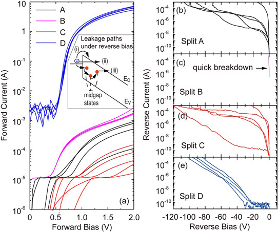
Figure 1: Plot of forward (a) and reverse current in diodes layers grown according to parameters (b) A, (c) B, (d) C and (e) D as function of bias voltage. Inset (a) shows three leakage paths under reverse bias.
The growth parameters D were used to create a 6μm lightly silicon-doped n-GaN drift layer with low carbon concentration. The n-type doping was around 1016/cm3. SBDs were fabricated with ion-implant edge termination and 0.8mmx0.8mm Schottky contacts. The overlap between the edge termination and contact was 10μm.
The resulting SBD achieved a breakdown of more than 800V for 1mA/mm2 (0.64mA) reverse leakage (Figure 2). The forward current at +2V was close to 1.6A and the specific on-resistance was around 5mΩ-cm2. The researchers claim the 0.77V turn-on voltage as among the lowest so far for GaN vertical diodes.
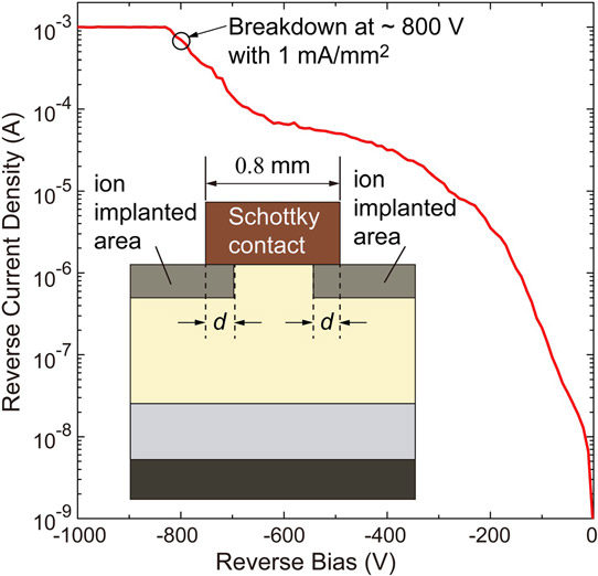
Figure 2: Plot of reverse leakage current in diode with 6μm GaN drift layer as function of bias. Inset: schematic of diode structure with isolation.
Through capacitance-voltage analysis, the researchers find a maximum electric field at breakdown of 1.38x10⁶V/cm at the Schottky/GaN interface. This value falls short of the theoretical value of 3.3x10⁶V/cm. "This means the breakdown is limited by the leakage through the barrier and could be further improved by enhancing the barrier height by surface treatment," the researchers comment.
GaN Schottky barrier diodes HRL MOCVD
http://dx.doi.org/10.1063/1.4941814
The author Mike Cooke is a freelance technology journalist who has worked in the semiconductor and advanced technology sectors since 1997.


