


- News
15 February 2016
HRL Laboratories claims first gallium nitride CMOS transistor fabrication
HRL Laboratories LLC in the USA claims the first demonstration of gallium nitride (GaN) complementary metal–oxide–semiconductor (CMOS) field-effect transistors [Rongming Chu et al, IEEE Electron Device Letters, published online 6 January 2016]. The team used the technology to create CMOS inverter circuits.
GaN is being developed for power switching and power microwave/millimeter-wave electronics. Present applications mostly use discrete transistors rather than integrated circuits (ICs). HRL sees a need for an IC approach to achieve the full benefits of GaN electronics at low cost. Parasitic inductance is one aspect that would be improved – discrete GaN components have to be slowed down to avoid voltage instability from chip-to-chip effects. ICs also have reduced assembly and packaging costs.
The CMOS processing began with metal-organic chemical vapor deposition (MOCVD) of the NMOS layers on sapphire (Figure 1). The Al0.25Ga0.75N top barrier was 5nm thick. The silicon nitride (SiN) encapsulation was 50nm.
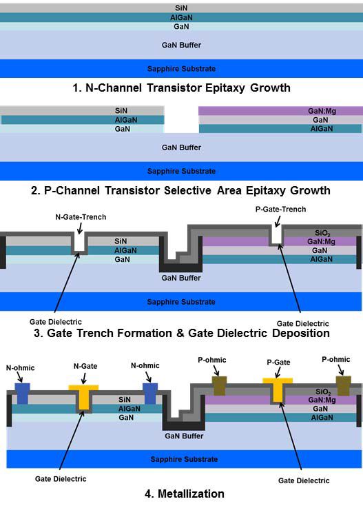
Figure 1: Major steps for fabricating GaN NMOS and PMOS on the same wafer.
The PMOS layers were applied by etching down to the GaN buffer in selected regions and MOCVD re-growth. The structure comprised a 30nm Al0.25Ga0.75N back barrier, 20nm of undoped GaN, and a 50nm magnesium-doped GaN hole supply layer.
Transistor fabrication began with ion implantation for device isolation, followed by gate trench low-energy plasma etch, AlN/SiN gate dielectric stack MOCVD, titanium/aluminium-based NMOS and nickel/gold PMOS ohmic source/drain formation, and nickel/gold gate electrode and interconnect deposition. The PMOS source/drain contacts were annealed in oxygen.
The researchers report that the NMOS and PMOS structures both exhibited enhancement-mode behavior in long-gate devices – i.e. normally-off at 0V gate potential, which is desired in power devices for fail safety and efficiency. The channel mobilities were 300cm2/V-s and 20cm2/V-s for NMOS and PMOS, respectively.
The researchers report that discrete NMOS devices with the same gate stack structure have achieved channel mobilities of more than 1000cm2/V-s. The team comments: "Further improvement of the GaN CMOS process is needed to improve the NMOS mobility to what was achievable with a discrete device process."
The PMOS mobility was higher than for bulk p-GaN (~10cm2/V-s) but lower than reported values for two-dimensional hole gases (2DHGs, ~40cm2/V-s). The researchers believe that PMOS improvements could come from "optimizing epitaxial re-growth, gate trench etch, and gate dielectric deposition".
Devices with 0.5μm and 75μm respective gate length and width had threshold voltages around 0V. For the NMOS device the on-resistance at +5V gate was 10Ω-mm. The PMOS on-resistance was much higher: 1314Ω-mm at -5V gate. The PMOS device also suffered from buffer leakage when the drain bias was greater than 2V. The researchers suggest that the leakage could be caused by parallel conduction at the MOCVD re-growth interface between the PMOS layer and the original GaN buffer.
The 0.5μm transistors were used in CMOS inverter circuits (Figure 2). The gate widths of the PMOS and NMOS transistors were 500μm and 50μm, respectively. The (differential) voltage gain was 9.6 at 1.2V input with 5V DC bias. The current drawn by the circuit (Idd) peaked at 1.5V input (Vin), where the inverter switched off.
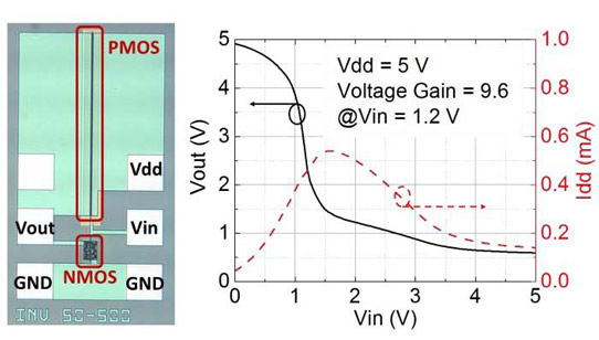
Figure 2: Microscope top-view photograph and measured voltage transfer curve of fabricated GaN CMOS inverter IC.
The researchers comment: "Thanks to the CMOS configuration, the Idd was considerably lower when the Vin was at 0V and 5V, suggesting low static power consumption. The static power consumption could be further decreased by reducing the off-state leakage of the NMOS and PMOS."
With 5V pulses with steps of 10ns rise/fall times, the output swung between 0V and ~5V with 90ns fall and 670ns rise.
The researchers comment: "Slower rise time is due to higher on-resistance of the PMOS. Although the performance is yet to be improved, the functional inverter IC proves the feasibility of the GaN CMOS technology."
http://ieeexplore.ieee.org/xpl/articleDetails.jsp?reload=true&arnumber=7373586
The author Mike Cooke is a freelance technology journalist who has worked in the semiconductor and advanced technology sectors since 1997.


