


- News
7 December 2016
Single III-V channel structure for complementary MOS transistors
Researchers based in Japan have developed a single ultrathin body (UTB) structure of indium arsenide and gallium antimonide on insulator (InAs/GaSb-OI) on silicon (Si) that can function as a complementary metal-oxide-semiconductor (CMOS) field-effect transistor (FET) [Masafumi Yokoyama et al, Appl. Phys. Lett., vol109, p213505, 2016].
The team from University of Tokyo, NTT Photonics Laboratories and JST-CREST achieved high channel mobilities in their devices.
Present proposals for CMOS electronics involving high-mobility III-V compound semiconductors such as InAs and GaSb use separate 'co-integrated' transistor structures for the n- and p-channel transistors. Alternatively, the co-integration involves InAs (or InGaAs) for the n-channel and germanium (Ge) for the p-channel devices. Co-integration is complex and would increase production costs.
The Tokyo/NTT/JST-CREST group proposes combining InAs and GaSb layers in a single structure on silicon. The type of conduction was controlled by a back-gate potential. The n-channel forms at gate-insulator/InAs interfaces, while the p-channel forms at GaSb/InAs interfaces. If the InAs layer is ultrathin, the hole mobility in the p-channel is enhanced due to size quantization, increasing the InAs energy gap to give insulating properties.
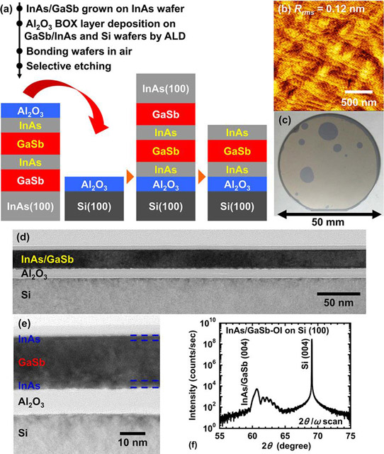
Figure 1: (a) Fabrication schematic of InAs/GaSb-OI on Si wafers. (b) Atomic force microscope (AFM) image of InAs/GaSb-OI on Si wafer surface with root-mean-square roughness (Rrms) of 0.12nm. (c) Photograph of 50mm-diameter InAs/GaSb-OI on Si wafer. (d and e) Transmission electron microscope (TEM) cross-sections. (f) X-ray diffraction spectra.
InAs/GaSb-OI layers were direct wafer bonded to (100) Si (Figure 1). The III-V layers were grown on InAs substrates. The bonding was made at room temperature in air between atomic layer deposition (ALD) aluminium oxide (Al2O3) layers on the III-V source and silicon wafers. Etching removed the InAs wafer and GaSb buffer layer, leaving the InAs/GaSb channel layers on the Al2O3 buried oxide insulator. X-ray analysis confirmed that the high crystal quality of the InAs/GaSb layers was maintained after the wafer bonding process.
Back-gate operation of an InAs/GaSb/InAs transistor with respective 2.5nm/20nm/2.5nm thicknesses gave a GaSb p-channel hole mobility of 159cm2/V-s. The researchers say this value exceeds that for silicon p-MOSFETs in the high-carrier-density region. An InAs n-channel of 5nm thickness gave an electron mobility of 1200cm2/V-s. Even with 2.5nm thickness the electron mobility, while lower, was still higher than UTB silicon-on-insulator devices with similar physical thickness, according to the team.
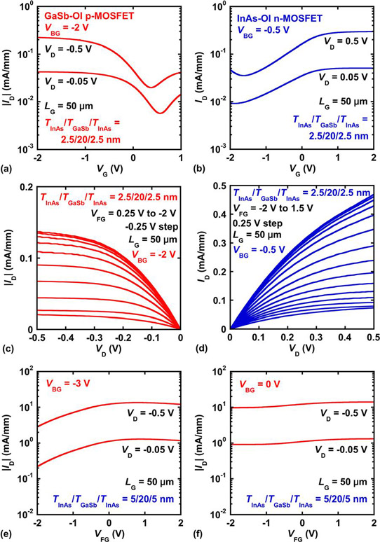
Figure 2: Front-gate operation of III–V CMOS InAs/GaSb-OI device with 2.5nm/20nm/2.5nm (a-d) or 5nm/20nm/5nm (e-f) InAs/GaSb/InAs layers with various back-gate potentials (VBG) to give p-MOSFET or n-MOSFET behaviors. Drain current (ID) plotted against (front) gate (VG/VFG) potential or drain bias (VD).
By using the back gate to set the p-/n-channel type of transistor, front-gate operation was also studied (Figure 2). A back-gate voltage of -2V was used for a GaSb-OI p-MOSFET and a voltage of -0.5V for an InAs-OI n-MOSFET. The InAs/GaSb/InAs structure was 2.5nm/20nm/2.5nm in both cases. Increasing the InAs layer thicknesses to 5nm created devices that were dominated by electron conduction: "Sufficient p-MOSFET operation cannot be achieved even under the strong hole accumulation condition with the negative back bias," the researchers report.
The team suggests that further optimization of InAs/GaSb thicknesses and transistor fabrication such as in the metal source-drain contact formation, along with improvement of InAs/GaSb channel material quality, could reduce off leakage current between source and drain. These factors could lead to CMOS operation with constant back-gate potential.
Also the off-current of the devices was too high for applications. Even if further refinement such as thinning the GaSb and InAs layers were not sufficient, the team suggests that the use of InGaAs and GaAsSb alloys could reduce the off-current by suitable adjustments of band offsets.
InAs/GaSb OI on silicon CMOS FET
http://dx.doi.org/10.1063/1.4968187
The author Mike Cooke is a freelance technology journalist who has worked in the semiconductor and advanced technology sectors since 1997.


