


- News
28 December 2016
Gallium nitride thin-film transistors produced in 200°C process
Bilkent University in Turkey has developed a low-temperature process to create gallium nitride (GaN) back-gated thin-film transistors (TFTs) on flexible and rigid substrates [S. Bolat et al, Appl. Phys. Lett., vol109, p233504, 2016]. The team reports that the "overall fabrication thermal budget is below 200°C, the lowest reported for the GaN-based transistors so far."
The Bilkent team points to potential applications of flexible devices for health monitoring, wearable electronics, and displays. Alternatives to the rigid TFT circuits used in most displays suffer from the need for high-temperature deposition/annealing steps. Organic and metal oxide devices are impacted by reliability issues. Although reliability in metal oxides such as zinc oxide can be improved with encapsulation, this adds to production complexity and cost.
Normally, GaN is deposited at high temperature around 1000°C, but other techniques such as atomic layer deposition have been developed with much improved thermal budget. "Up to now, the nitride-based electronic and optoelectronic devices have been realized on flexible substrates only via the transferring method, which carries the potential risk of decreasing the yield of the devices, which therefore prevents the commercialization of the proposed devices," the team writes.
The Bilkent researchers say that they have beaten their own record for lowest-temperature GaN electronic devices. The present results are not exactly high performance, but the team hopes that III-nitride-based flexible electronics could follow from further materials and process optimization.
The researchers produced GaN TFTs (Figure 1) on rigid p-type silicon and flexible polyethylene naphthalate (PEN). Hollow-cathode plasma-assisted atomic layer deposition (ALD) at 200°C was used to create 77nm aluminium oxide (Al2O3) and 11nm GaN layers on a silicon dioxide layer in which patterned windows were cut to define the devices. The 200nm silicon dioxide was created by electron-beam evaporation.
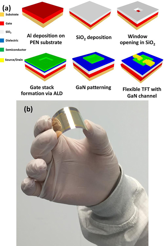
Figure 1: (a) Schematic of device fabrication steps on flexible substrate, and (b) photograph of flexible substrate with series of bottom-gated TFTs with GaN channels flexed in author's hand.
The silicon dioxide was applied directly to cleaned rigid silicon substrates. For PEN substrates, a 100nm aluminium layer formed a back-gate structure on which the silicon dioxide was applied. In the rigid-substrate devices, the back gate was formed by p-silicon.
The devices consisted of square gates with 50μm length and width. Device isolation was by dry etch. The source/drain contact metals were titanium/gold.
The devices on rigid substrates achieved on/off current ratios of 2x10³ with "clear saturation in their output characteristics". The threshold voltage was +0.25V. The effective mobility was 0.005cm2/V-s with 10V gate potential and 1V drain bias. The low mobility is blamed on "the nanocrystalline and defective nature of the ALD-based GaN thin films".
On flexible substrate, the TFT managed a reduced on/off ratio of 7x10², while giving a higher threshold voltage of +2.5V (Figure 2). The researchers comment: "The difference in the threshold voltage can be attributed to the higher oxygen concentration in the as-deposited GaN thin films on flexible substrates (10% oxygen) compared to rigid substrates (2–3% oxygen), which is confirmed with the x-ray photo-spectroscopy measurements."
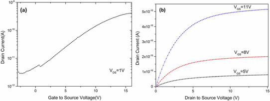
Figure 2: (a) Transfer and (b) output characteristics of GaN TFTs on flexible substrates.
The higher oxygen content results in the formation of Ga2O3 in the GaN thin film; "therefore the devices on the flexible substrate demonstrate a higher threshold voltage and lower on-to-off current ratio," the researchers write.
The effective mobility on flexible substrate was 0.0012cm2/V-s with 8V gate potential and 1V drain bias.
Gate-bias stability of the flexible TFTs under 10V stress with source and drain grounded for varying periods was tested. The 10V gate bias represented an electric field of 1.3MV/cm in the gate oxide. The threshold voltage shift after 1000 seconds was 0.14V (~5%). This compares with ZnO-based TFTs that have a shift of 11V under the same conditions.
The researchers comment: "This result is significantly important in the sense that no encapsulation or annealing, which are commonly applied methods to electrically stabilize the TFTs with semiconducting metal oxide channels, are needed to stabilize the devices."
http://dx.doi.org/10.1063/1.4971837
The author Mike Cooke is a freelance technology journalist who has worked in the semiconductor and advanced technology sectors since 1997.


