


- News
11 August 2016
Disco develops laser ingot slicing method to speed SiC wafer production and cut material loss
Tokyo-based equipment maker Disco Corp has developed the KABRA (Key Amorphous-Black Repetitive Absorption) laser ingot slicing method. Implementing the process is said to enable high-speed production of silicon carbide (SiC) wafers, increase the number of wafers produced from a single ingot, and dramatically improve productivity.
Existing methods for slicing wafers from a silicon carbide ingot mainly use multiple diamond wire saws for mass-producing wafers because the processing time is long due to the high rigidity of SiC. The number of wafers produced from a single ingot is also small due to the large amount of material lost in the slicing sections. This has been a major factor that increases the cost of producing SiC power devices, hindering their introduction to the market and the widespread use of SiC power devices, says Disco.
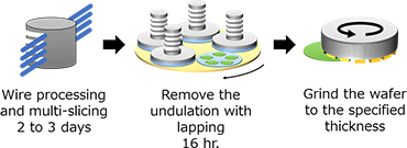
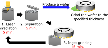
Figure 1: Comparison of processing time between existing process (top) and KABRA process (bottom) when producing a specified thickness of 350µm from 4"-diameter 20mm-thick SiC ingot. (Existing process: general values based on user info.)
The KABRA process forms a flat light-absorbing separation layer at a specified depth through irradiation with a continuous, vertical laser from the upper surface of the SiC. Conventional laser processing is not suitable for slicing, says Disco, because the modified layer formed by laser irradiation, in principle, extends in the direction of the laser incident – see Figure 2(a). However, Disco's new laser slicing method focuses on two facts: (1) SiC can be decomposed by focused continuous laser irradiation and separated into amorphous silicon (Si) and amorphous carbon (C) in an amorphous state; and (2) the light absorption coefficient is about 100,000 times larger than that of SiC.
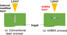 Figure 2: Difference of modified layer forming direction.
As a result, Disco forms KABRA layers inside the ingot both vertically and in the direction of the laser incidence, establishing what is claimed to be the optimal laser slicing method - see Figure 2(b). In addition, the patent-pending process can be applied to various types of SiC ingots, including single-crystal (4H, 6H, and semi-insulation) and multi-crystal ingots.
One of the major characteristics is that the process can be applied to monocrystal ingots, regardless of the off-angle of the crystal c-axis.
Disco says that other advantages of the process include the following:
- Processing time is greatly reduced
Existing processes require about 2 hours to slice a wafer from a 4"-diameter SiC ingot, and 2-3 days for one ingot (when producing a specified thickness of 350µm from a 4"-diameter 20mm-thick SiC ingot). In contrast, the KABRA process can greatly reduce the processing time, it is claimed, requiring only 25 minutes to slice a wafer (about 18 hours for one ingot) in total processing time (including laser irradiation, separation, and ingot grinding). In addition, the process only takes about 30 minutes to slice a wafer from a 6"-diameter SiC ingot, even though the existing process requires over 3 hours. - Lapping process is no longer required
For wire processing, a lapping process is required to remove about 50µm of undulations generated on the surface of a processed wafer. However, the KABRA process does not require lapping because the wafer undulation after separation can be controlled (Figure 2), making it possible to greatly reduce the initial costs and running costs. - Number of wafers produced increases by 1.5 times that of existing processes
Although wire processing produces about 200µm of material loss per wafer at the slicing sections (kerf loss), the KABRA process essentially has no material loss. In addition, the removal amount of the KABRA layer after separation can be suppressed to about 100µm. This increases the number of wafers produced from a single ingot by about 1.5 times that of the existing process.
Disco is now accepting requests for test cuts, and plans a chargeable processing service. The firm will also give academic conference presentations at The Japan Society for Precision Engineering Autumn Meeting/The Japan Society of Applied Physics Autumn Meeting in September 2016, and will exhibit the KABRA equipment for the first time at the SEMICON Japan 2016 trade show (14-16 December).


