


- News
22 September 2015
Tunnel junction for vertical-cavity surface-emitting laser
University of California Santa Barbara (UCSB) has developed an n-type gallium nitride (n-GaN) tunnel junction (TJ) intracavity contact to reduce threshold current and increase differential efficiency in its m-plane III-nitride vertical-cavity surface-emitting laser (VCSEL) design [J. T. Leonard et al, Appl. Phys. Lett., vol107, p091105, 2015].
VCSELs can be fabricated in two-dimensional arrays and can emit highly directional high-power radiation. Potential applications for III-nitride VCSELs include atomic clocks, gyroscopes, magnetometers, and visible light communication.
The VCSEL structure produced by metal-organic chemical vapor deposition (MOCVD) on m-plane free-standing GaN substrates was similar to previous UCSB work, although the number of quantum wells was reduced from ten to seven [Click to view]. The device was mounted on a copper block with titanium/gold coating.
The ~141nm n-GaN TJ intracavity contact was produced by ammonia molecular beam epitaxy (MBE). At present MOCVD TJs have high resistance. The advantage of MBE is lower hydrogen levels during growth, compared with MOCVD. Hydrogen passivates MOCVD p-GaN layers reducing carrier concentrations.
Before growth of the TJ, the p-GaN of the MOCVD epitaxial structure was activated, followed by mesa etch and aluminium ion implant to create the aperture. The junction itself consisted of four alternate layers of heavily doped and normally doped n-GaN with thicknesses of 39.6nm except for one of the normally doped layers being 22.1nm. The structure was designed to reduce free-carrier absorption by aligning the heavily doped layers with nodes of the radiation field.
A comparison device used an indium tin oxide (ITO) transparent contact with an 1/8th-wave tantalum pentoxide (Ta2O5) spacer. The purpose of the spacer was to position the node of the radiation field in the ITO to reduce absorption.
The distributed Bragg reflectors (DBRs) on the n- and p-sides consisted of layers of tantalum pentoxide and silicon dioxide.
The threshold current of the TJ VCSEL was much reduced – 3.5kA/cm2 (4mA), compared with 8kA/cm2 (9mA) for the ITO structure (Figure 1).
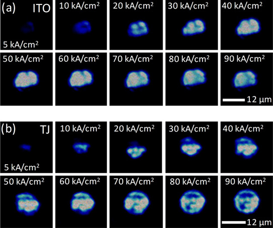
Figure 1: Voltage, light output power versus current characteristics of TJ VCSEL and ITO VCSEL measured under pulsed operation (0.3% duty cycle, 100ns pulse width).
The researchers report: "Both devices were designed to lase at 405nm; however, a Ta2O5 spacer was accidentally deposited on the n-side of the devices, which shifted the cavity resonance wavelength to 410nm and 417nm for the ITO and TJ VCSEL, respectively. It is of note that this may have also led to a misalignment of the peak gain and the cavity resonance wavelengths, which can lead to an increase in the threshold current density."
The differential efficiency increased to 0.262% from 0.062% for the TJ and ITO VCSELs, respectively. The researchers suspected filamentary lasing, since these values are much lower than simulations predicted. Indeed, this was confirmed by microscopic inspection of the near field (Figure 2). With filamentation, large areas of the material do not contribute to lasing, reducing efficiency.
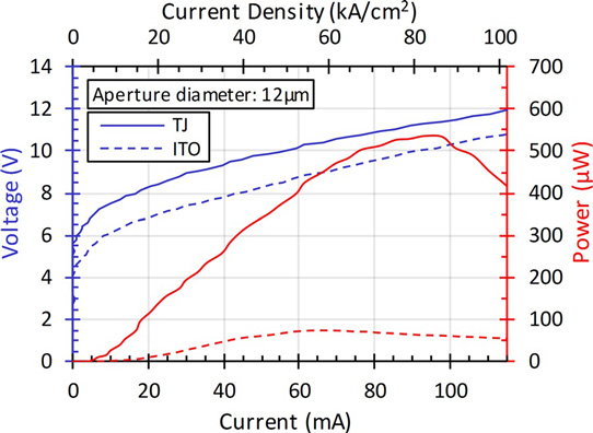
Figure 2: Optical microscope images taken under low gain to prevent detector saturation: (a) shows ITO VCSEL, while (b) shows TJ VCSEL operating at various current densities. Both cases exhibit filamentary lasing in aperture. Non-circular emission pattern in ITO case is result of partial over-etching during top-down photo-electro-chemical etch.
The researchers comment: "We suggest that filamentary lasing may be predominantly related to variations in contact resistance and non-uniform current spreading, both of which may then create local variations in the refractive index and free-carrier absorption."
One drawback in the use of a TJ contact was an increase in the forward voltage by about 1.5V over that of the ITO device. The researchers believe an improved surface treatment before the MBE re-growth could reduce this forward voltage penalty by 0.5V-1.0V.
VCSEL n-GaN GaN substrates MOCVD MBE
http://dx.doi.org/10.1063/1.4929944
The author Mike Cooke is a freelance technology journalist who has worked in the semiconductor and advanced technology sectors since 1997.


