


- News
11 September 2015
Increasing carrier lifetimes for high-voltage silicon carbide
Researchers in Japan have been developing ways to increase minority carrier lifetimes in lightly doped silicon carbide (SiC) with a view to insulated-gate bipolar transistors (IGBTs) [Tetsuya Miyazawa et al, J. Appl. Phys., vol118, p085702, 2015]. Such devices are being developed to handle very high voltages beyond 10kV for electric power transmission and distribution.
To handle high voltages, devices need a low resistance but relatively thick drift layer. The resistance of the drift layer is adversely affected by the short minority carrier lifetime typically achieved with SiC, particularly p-type. However, devices with n-type drift layers suffer from the high resistance of p-type substrates.
The team from Central Research Institute of Electric Power Industry (CRIEPI), Kansai Electric Power Co Inc, and National Institute of Advanced Industrial Science and Technology explored ways to create structures for both p- and n-type IGBTs to overcome these drawbacks.
A vertical hot-wall chemical vapor deposition (CVD) reactor was used for epitaxy on 3-inch 4H silicon-face n+-SiC with 4° offcut for both devices. Silane and propane were the silicon and carbon sources, respectively. The carrier gas consisted of hydrogen and hydrogen chloride. The p- and n-type dopants were trimethyl-aluminium and nitrogen, respectively.
Particular care was needed to control the TMA delivery for low-concentration p-type doping (~1014/cm3) and the researchers developed a modified feed system that involved diluting the hydrogen containing the TMA with more hydrogen before delivering it to the CVD reactor.
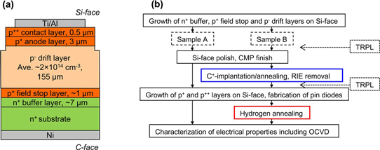
Figure 1: (a) Schematic cross-section and (b) fabrication process of simple PiN diode with Si-face p-IGBT structure (p-PiN).
A structure suitable for a p-IGBT (Figure 1) was grown first up to a 180μm p- drift layer that was subsequently trimmed back to 155μm by chemical mechanical polishing (CMP). Carrier lifetime enhancement was achieved for some devices (sample B) by carbon implantation to a depth of 250nm and annealing in argon. The surface was protected with a carbon cap that was later removed by ashing. The implanted region was also removed by reactive ion etch (RIE) of a 1μm layer.
PiN diodes were fabricated as test vehicles for the structure and related processing by growing and p+ anode and p++ contact layers. The devices were fabricated with 4mmx4mm mesas. After contact metal deposition the devices were then singulated into chips. Sample B devices were also subjected to hydrogen annealing at 800°C for 10 minutes between contact metal deposition and singulation.
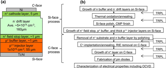
Figure 2: (a) Schematic cross-section and (b) fabrication process of simple PiN diode with C-face n-IGBT structure (n-PiN).
Structures for n-IGBTs (Figure 2) were achieved using an inverted growth process on an n+ substrate. The growth began on the silicon-face to create a buffer and 180μm n- drift layer. A first carrier lifetime enhancing process consisted of thermal oxidation and annealing. Before further growth of the field stop and p-type layers, the surface was planarized with CMP.
The substrate and n-type buffer were removed by polishing, leaving a 160μm drift layer with a carbon-face on a free-standing structure. The structure suffered from significant physical distortion (increased 'SORI') due to the removal of the substrate.
Further carrier lifetime enhancement consisted of carbon implantation, annealing and removal, as for the p-IGBT structure. PiN devices were produced by growing a 5μm n+ layer on the carbon-face drift layer and applying contacts as with the p-PiN diodes.
For the p- drift layer, the effect of the carbon implantation and annealing was to increase the minority carrier lifetime from 3.0μs to 5.6μs, according to time-resolved photoluminescence (TRPL). Even the untreated lifetime of 3.0μs is longer than typical for p- SiC. The researchers attribute this to special measures taken to avoid carbon vacancy defects, and to the very low aluminium doping concentration.
The carbon vacancies were reduced by changing the growth temperature and C/Si ratio for the buffer (>1650°C, 0.75) and drift layer (~1600°C, 0.94-1.00) growth. The higher growth temperature and lower C/Si for the buffer avoided triangular defects indicative of 3C-polytype inclusions.
After the thermal oxidation and annealing, the 155μm drift layer had a minority carrier lifetime of 5.1μs, according to differential microwave photoconductance decay measurements.
For the n- drift layer the minority carrier lifetime was increased from 7μs to 24μs by the carbon implantation and anneal. The growth conditions for the drift layer were 1610°C and C/Si ratio of 1.00.
The p-PiN diodes had a voltage drop of more than 10V for the flow of 10A/cm2 at room temperature. The performance improved at 200°C with a voltage drop of 3.5V with 100A/cm2 current for sample B material (extended minority carrier lifetime). The drop for sample A without carbon implant and anneal treatment was 5.7V for the same current. The differential on-resistance was 22mΩ-cm2 and 4.2mΩ-cm2, respectively, for samples A and B. Sample B devices without the final hydrogen anneal had a higher voltage drop of 4V.
Open-circuit voltage decay (OCVD) measurements on sample B showed an increase in minority carrier lifetime from 5μs at room temperature to 44μs at 250°C, which the researchers say is exceptionally long for a p-type epilayer.
Table 1: TRPL minority carrier lifetimes of n- thick drift layer of n-PiN.
| Minority carrier lifetime (μs) | |
| After thick n- epitaxial growth | 3.2 |
| After thermal oxidation/anneal process | 10.0 |
| After removal of n+ substrate | 8.2 |
| After C+-implantation/anneal process | 10.7 |
The TRPL results for the n-PiN growth sequence (Table 1) showed the final structure as having a minority carrier lifetime of 10.7μs. The n-PiN had a much lower voltage drop at room temperature of 5.5V for 100A/cm2 current. Increasing the temperature reduced the voltage drop to less than 3.0V at 250°C. The differential on-resistance was 17mΩ-cm2 at room temperature and 1.9mΩ-cm2 at 250°C.
Decreasing the device area to 1.0mmx1.0mm increased the voltage drop to the range 6.5V-8.0V. The researchers attribute this to carrier recombination at the mesa periphery. Surface passivation to reduce this effect should improve performance.
http://dx.doi.org/10.1063/1.4929456
The author Mike Cooke is a freelance technology journalist who has worked in the semiconductor and advanced technology sectors since 1997.


