


- News
2 September 2015
Forward-bias gate breakdown in HEMTs with enhancement-mode p-GaN gate
Researchers in Belgium have studied forward gate breakdown of enhancement-mode aluminium gallium nitride/gallium nitride (AlGaN/GaN) high-electron-mobility transistors with p-type GaN gate electrodes [Tian-Li Wu et al, IEEE Electron Device Letters, published online 05 August 2015]. The team from imec, KU Leuven, and Centre for Microsystems Technology (CMST) comments: "To the best of our knowledge, it is the first time that the temperature dependency of the forward gate breakdown has been characterized."
Somewhat unexpectedly, the research found a positive temperature dependence where a higher temperature leads to a higher gate breakdown voltage.
Enhancement-mode, normally-off transistors are preferred for the target application of power switching. Without special processing, AlGaN/GaN HEMTs are depletion-mode, normally-on. Enhancement-mode should give fail-safe operation and low power consumption. The use of p-GaN in the gate stack is one promising approach for shifting AlGaN/GaN HEMTs to enhancement-mode operation.
AlGaN/GaN HEMTs with p-GaN gates have not been extensively studied from stability and reliability perspectives. Gate breakdown is an important aspect of such assessments that up to now has not been intensively reported.
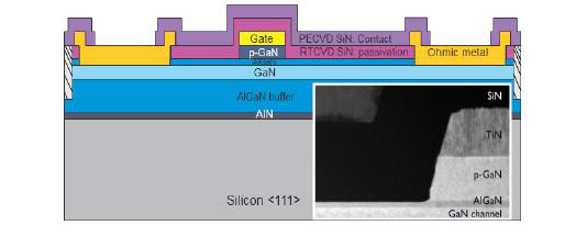
Figure 1: Schematic cross-section of Schottky metal/p-GaN gate AlGaN/GaN HEMT and TEM picture of gate region (inset).
The epitaxial material for the HEMT (Figure 1) consisted of 2.4μm (Al)GaN buffer, 300nm GaN channel, 15nm AlGaN barrier, and 70nm magnesium-doped p-GaN. The substrate for the metal-organic chemical vapor deposition (MOCVD) was 200mm-diameter silicon (111). (Al)GaN was used for the buffer to enable high-voltage operation.
The gate consisted of a titanium nitride electrode on the p-GaN, forming a Schottky contact. After the gate metal was deposited, a selective etch with silicon nitride masking the gate structure was carried out down to the AlGaN barrier. The silicon nitride mask was removed before depositing silicon nitride passivation. Finally, the gold-free ohmic contacts, along with interconnects, were formed. The metallization included a thick power line.
The gate length was 0.7μm. The gate-drain and gate-source distances were both 0.75μm. The gate width was 10μm.
The threshold voltage was +1.6V, giving enhancement-mode, normally-off operation. With 8V gate potential and 1V drain bias, the drain current was 90mV/mm and the gate leakage 5x10⁻⁷mA/mm. The subthreshold swing was 90mV/decade.
The gate hard breakdown characteristics were measured at 0V drain bias at temperatures up to 200°C. Each measurement used a fresh device. The results for the four measurement temperatures (25°C, 75°C, 150°C, 200°C) consisted of averages over 15 devices. The gate breakdown voltage increased with temperature at the rate of +5x10⁻³V/°C – a +1V difference between 25°C and 200°C (Figure 2).
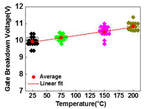 Figure 2: Gate breakdown voltage versus temperature. Voltage extracted at 10-3mA/mm leakage current.
Such a positive dependence has never been seen with metal-insulator-semiconductor AlGaN/GaN HEMTs. However, such behavior is seen in silicon CMOS transistors and depletion-mode (normally-on) AlGaN/GaN HEMTs. In these cases, the mechanism for gate breakdown is thought to be avalanche breakdown triggered by impact ionization. GaN pn diodes under reverse bias also breakdown by this mechanism.
The researchers comment: "This suggests that such a positive temperature forward gate breakdown characteristic we observed first time on Schottky metal/p-GaN gate AlGaN/GaN HEMTs could be related to avalanche breakdown as well."
The team explains, further: "Such a gate breakdown phenomenon can be explained by avalanche multiplication in the space charge region of the Schottky metal/p-GaN junction. Once the electrons transfer to the p-GaN region, they can be accelerated by a high electrical field in the depletion region, yielding impact ionization."
The researchers also observed luminescence when the gate voltage was close to hard breakdown. Such light emission is indicative of avalanche luminescence from impact ionization, although some of the photons could also come from band-to-band transitions.
AlGaN/GaN HEMTs GaN HEMTs p-type GaN gate electrodes MOCVD
http://ieeexplore.ieee.org/xpl/articleDetails.jsp?arnumber=7180329
The author Mike Cooke is a freelance technology journalist who has worked in the semiconductor and advanced technology sectors since 1997.


