


- News
15 October 2015
SiC, GaN and other wider-bandgap materials present new choices for power electronics
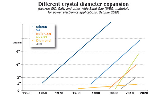
When people think about wide-bandgap (WBG) semiconductor materials for power electronics applications, they usually think of gallium nitride (GaN) or silicon carbide (SiC) – which is not surprising, since SiC and GaN are currently the most advanced WBG technologies for power electronics applications. However, market research firm Yole Développement notes in its report 'SiC, GaN, and other Wide Band Gap (WBG) materials for power electronics applications' that there are materials with an even larger bandgap that can further increase power device performance:
- Due to its high bandgap and possibility of doping at room temperature, gallium oxide (Ga2O3) has been proposed for power electronics applications. Compared to existing SiC and bulk GaN technology, its key selling point is the possibility of using melt growth to make large, inexpensive wafers.
- Diamond is the ideal candidate for power electronic applications, thanks to a combination of unique properties.
- Having initially targeted ultraviolet (UV) LED applications but finding subpar demand, some aluminium nitride (AlN) suppliers are now targeting the power market in order to diversify their activities. AlN's key value proposition for power applications is the fact that it has the largest band gap.
SiC n-type wafers to grow at 21% CAGR to $110m by 2020
Driven by the SiC-based power devices market, the market for n-type SiC substrates is expected to rise at a compound annual growth rate of 21% from about $35m in 2014 to $110m in 2020.
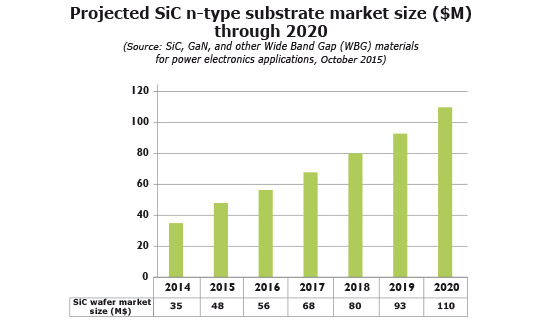
The market's preferred product for power electronic applications is still 4" wafers. However, some suppliers can now provide 6" wafers with good enough quality for power devices - and an 8" SiC wafer was demonstrated by II-VI Inc towards mid-2015.
The average price for 6" is still 2.25x higher than 4", but the price continues to fall and will drop below the threshold in late 2015 or early 2016. The transition to 6" is beginning; in fact, SiC device maker Rohm has just announced that it is beginning mass production on 6" wafers in third-quarter 2015.
The n-type SiC substrate market player rankings have recently stabilized, says Yole. Cree remains the market leader, with Dow Corning, SiCrystal and II-VI right behind. There are now four Chinese SiC suppliers, and their current announced capacity is more than 150,000 wafers per year, with further increases expected. Also, in early 2015 Beijing-based TankeBlue Semiconductors demonstrated a 6" n-type wafer. Yole views these Chinese players as serious market challengers.
Many players competing on GaN-on-Si epiwafer open market. What will happen?
GaN-on-silicon technology is very challenging due to large in mismatches both the lattice constants and coefficients of thermal expansion (CTE) between GaN and silicon. That said, GaN-on-Si's main issues have been resolved and several companies have begun commercializing power devices based on this technology, notes Yole.
Attracted by the device market's potential, players with different origins are active on the open market for GaN-on-Si epiwafers and thinking of selling epiwafers to device players. These players are:
- silicon substrate suppliers wanting to move up the value chain, i.e. Siltronic;
- device foundries like Episil that want to move down the value chain;
- some LED chip suppliers, i.e. China's San'an Optoelectronics;
- large epi houses like IQE;
- Epigan and other pure GaN epi houses.
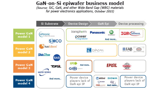
Since the power GaN device business is only in its early stages, the related GaN epiwafer open market is not yet well-established, notes Yole. Competition is very intense, and the bankruptcy of AZZURRO Semiconductors of Dresden, Germany in 2014 has illustrated the risks faced by start-up GaN epi houses.
The report includes a detailed description of the GaN-on-Si epiwafer market and Yole's vision for its future.
Status of bulk GaN wafer production
Almost all commercial bulk GaN wafers are produced by hydride vapor phase epitaxy (HVPE), used mainly for optoelectronics applications. However, HVPE GaN substrates have an undesirably high dislocation density that restricts their usefulness for power switches, Yole notes.
Ammonothermal growth is expected to be more competitive with the arrival of a new acidic ammonothermeral method developed by Japan's Mitsubishi Chemical and US-based LED maker Soraa. Na-flux LPE growth also seems to be promising for power electronics devices, adds the market research firm.
The bulk GaN wafer market is dominated by Japanese companies. Sumitomo Electric, Mitsubishi Chemical, and Hitachi Metals (now Sumitomo Chemical) lead in HVPE production. Mitsubishi is actively developing ammonothermal growth, while NGK is developing Na-flux growth. Non-Japanese players are currently in small-volume production or in the R&D stage, and most of them are developing HVPE methods to target the LED market. If GaN-on-GaN technology is adopted by the power electronics market, Japanese players will maintain their leading position, reckons Yole.
The report also provides information on the alternative solutions being proposed to produce much cheaper bulk GaN and SiC wafers, which could potentially disrupt the GaN and SiC market, concludes Yole.
SiC market to treble and GaN to explode - if challenges are overcome
Power electronics SiC GaN-on-SiC GaN-on-Si Bulk GaN GaN substrates
www.i-micronews.com/component/hikashop/product/


