


- News
11 November 2015
Suppressing current collapse in normally-off gallium nitride transistor
Japan's Panasonic Corp has reported the suppression of current collapse up to 800V for a normally-off gallium nitride (GaN) transistor by embedding a hybrid drain in a gate-injection transistor (HD-GIT) structure [Kenichiro Tanaka et al, Appl. Phys. Lett., vol107, p163502, 2015].
The hybrid drain consists of a normal drain and an addition p-type drain with p-GaN deposited on the aluminium gallium nitride (AlGaN) barrier layer. The two drain regions are connected. The researchers see applications as next-generation power transistors for efficient, reliable high-power switching.
Current collapse in GaN transistors describes current reduction when the device is subjected to switching, compared with direct current measurements. Such effects are related to charge-trapping that affects the dynamic performance.
In Panasonic's GITs, current collapse has been attributed to emission of holes in the epilayer during off states. The p-drain injects holes into trapping states in the off condition so that they become inert.
The device material was grown on silicon (Figure 1). Unlike high-electron-mobility transistors (HEMTs), the structure includes a p-GaN top layer that is formed on a recessed AlGaN barrier layer. The p-GaN is used to create the gate of the GIT and the p-GaN hybrid drain. The researchers comment: "The entire structure is designed to eliminate the carrier traps and to reduce the internal electric field."
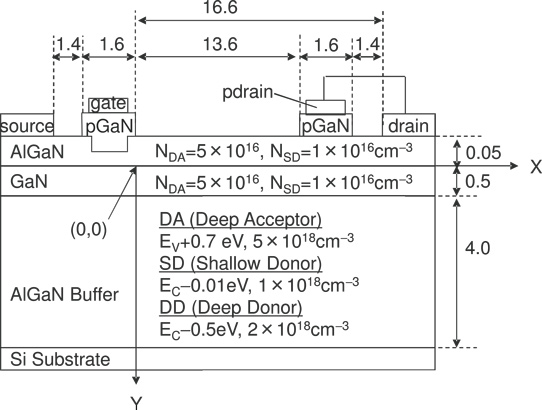
Figure 1: Schematic of HD-GIT. Device dimensions indicated in μm. Energy levels and concentrations of traps employed in simulation also shown.
The threshold voltage for the HD-GIT was 1V. Further, the specific on-resistance was 60mΩ and breakdown occurred at 1000V with a grounded silicon substrate.
In pulsed operation, the dynamic on-resistance remained near 60mΩ up to 800V (Figure 2). A comparison GIT device, by contrast, began to show increased dynamic on-resistance above 550V.
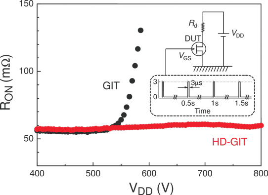
Figure 2: Dynamic ON-state resistance RON (t = 3μs) of HD-GIT and GIT as function of applied voltage VDD. Inset: circuit used in switching measurement.
The researchers comment: "This indicates that the introduction of the p-drain in the HD-GIT helps inject holes at the OFF state and suppress the current collapse effectively."
Simulations suggest that hole injection from the p-drain prevents the gate/p-drain access region from being negatively charged due to hot electrons, according to the researchers. They add: "At the OFF state, the hole injection from the p-drain prevents the gate/p-drain access region from being negatively charged by occupying the deep level in the epilayer. This results in the linear conduction band energy profile at the gate/p-drain access region. It also leads to flat potential right after turning ON, resulting in the complete suppression of the current collapse."
Panasonic GaN transistor GaN AlGaN
http://dx.doi.org/10.1063/1.4934184
The author Mike Cooke is a freelance technology journalist who has worked in the semiconductor and advanced technology sectors since 1997.


