


- News
6 November 2015
II-VI semiconductor green laser diode achieves lower current threshold
Jijun Feng and Ryoichi Akimoto based in China and Japan have developed low-threshold green and green-yellow laser diodes (LDs) based on a beryllium zinc cadmium selenide (BeZnCdSe) quantum well [Appl. Phys. Lett., vol107, p161101, 2015]. Feng comes from China's University of Shanghai for Science and Technology, and both researchers are associated with Japan's National Institute of Advanced Industrial Science and Technology (AIST).
Feng and Akimoto are seeking to plug the 'green gap' for laser diodes, giving access to display and projector applications. Alternative green-emitting materials such as indium gallium nitride (InGaN) lead to laser diodes with high thresholds and stability problems. Low thresholds can be achieved for blue-green ZnSe, but device lifetimes tend to be short.
Adding beryllium should improve the lifetime by shifting the chemical bonds from highly ionic towards a more covalent character. Previously, BeZnCdSe single quantum well (SQW) laser diodes have achieved 545nm wavelengths. Feng and Akimoto have created laser diodes with even longer wavelengths – green and green-yellow devices emitting ~535nm and ~560nm, respectively.
Molecular beam epitaxy (MBE) on gallium arsenide (GaAs) was used to create the lasing material (Figure 1). Zinc chloride and nitrogen RF-activated plasma were used to give n- and p-type doping, respectively. Separate chambers were used for III-V (GaAs buffer) and II-VI growth. The BeTe buffer was designed to protect the GaAs buffer surface from Ga2Se3 formation, which causes stacking faults.
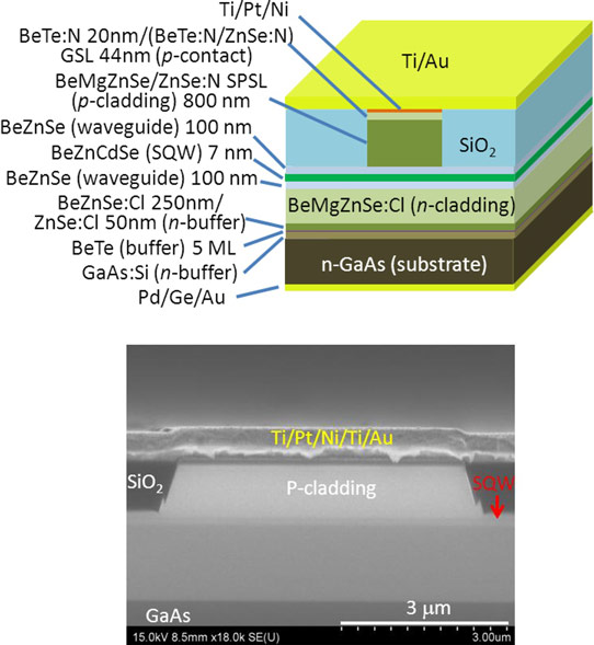
Figure 1: (a) Schematic of BeZnCdSe SQW LD. (b) Cross-sectional scanning electron microscope image of fabricated waveguide LD.
A separate-confinement heterostructure was used with Be0.02Zn0.68Cd0.30Se single quantum well between Be0.03Zn0.97Se optical guiding layers. The n-cladding was Be0.06Mg0.06Zn0.88Se. The p-cladding consisted of a short-period superlattice (SPSL) of 6x(Be0.10Mg0.14Zn0.76Se/ZnSe). The p-contact consisted of a BeTe/ZnTe pseudo-graded superlattice, where the thickness of the layers is varied.
The ridge waveguide was dry etched using a metal mask of titanium/platinum/nickel that also served as the ohmic p-contact. The ridge was buried with silicon dioxide from plasma-enhanced chemical vapor deposition (PECVD). The structure was finally planarized with chemical mechanical polishing (CMP). A final titanium/gold metal p-electrode was deposited, making contact with the p-ohmic metals, and then the n-contact metals were evaporated onto the back-side of the wafer.
The cavity length was defined by cleaving the device wafers. The facets were coated with a ~90% reflective dielectric structure of four pairs of silicon dioxide and zirconium dioxide layers from electron cyclotron resonance plasma-enhanced sputtering.
The devices were mounted p-side down on ceramic aluminium nitride heat-sinks with gold/tin eutectic bonding.
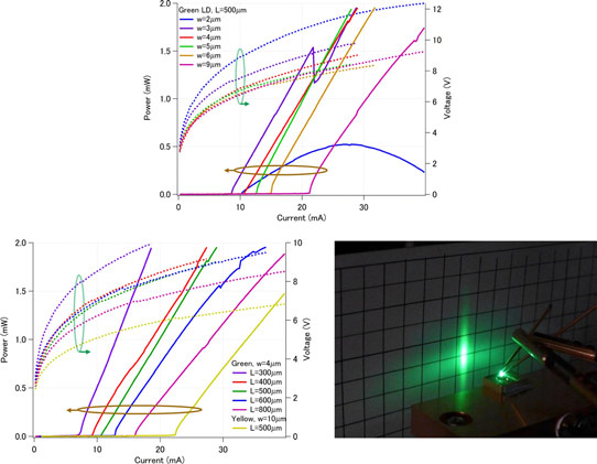
Figure 2: (a) Light output power and voltage–current characteristics with varying mesa width for 500μm-long laser diodes under cw operation at room temperature (25°C). (b) Lasing performance with varying mesa length. (c) Lasing image of 4μm-wide, 500μm-long laser diode with 20mA current. Monitor screen with 5mm-period grid was placed about 10mm before laser diode.
Under continuous-wave (cw) operation (Figure 2), there is a trade-off between current threshold and lifetime with narrower ridges giving lower thresholds but short time to burn-out from overheating. Green laser diodes with 4μm ridges and 300μm cavity length had current and voltage thresholds of 7.07mA and 7.89V, respectively. The power/current slope efficiency was 0.16W/A per facet. The threshold current represents a 10-fold reduction from previous work giving 68mA (AIST/Hitachi/Sony).
The green-yellow laser diode with a 10μm-wide ridge and 500μm cavity had thresholds of 21.18mA and 6.024V, improving on 94mA and 9.6V in previous work (AIST/Hitachi).
The researchers attribute the improved threshold to more vertical current flow with suppression of lateral carrier spreading.
The series resistance of device is described as "slightly high". The researchers suggest that optimizing the p-doping of the SPSL could reduce the resistance. Further improvements could come from quadratic grading, for instance, of the ZnSe/BeTe pseudo-graded superlattice, giving a smooth potential profile for hole injection. Doping the optical waveguide layers could also reduce resistance.
Laser diodes BeZnCdSe quantum well MBE GaAs substrate
http://dx.doi.org/10.1063/1.4934359
The author Mike Cooke is a freelance technology journalist who has worked in the semiconductor and advanced technology sectors since 1997.


