


- News
21 May 2015
Vertical gallium nitride transistors with buried p-type current blocking
University of California Santa Barbara (UCSB) and Arizona State University in the USA have developed gallium nitride (GaN) Current Aperture Vertical Electron Transistors (CAVETs) with a buried p-type layer, creating a reverse-biased pn junction [Ramya Yeluri et al, Appl. Phys. Lett., vol106, p183502, 2015].
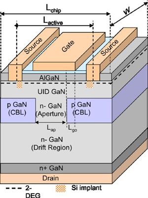 Figure 1: CAVET schematic with AlGaN/GaN heterojunction channel, p-GaN current-blocking layer (CBL) and aperture layer, and n-GaN drift region.
The CAVET (Figure 1) combines both a two-dimensional electron gas (2DEG) and a vertical structure. The 2DEG near the aluminium gallium nitride/gallium nitride (AlGaN/GaN) interface offers high conductivity, while the vertical structure should allow better electric field distribution with lower peak values.
In lateral GaN transistors such as high-electron-mobility transistors (HEMTs) the electric field peaks near the surface layer. Charging and discharging of surface states in lateral devices causes current collapse and other performance dispersion in pulsed operation. Also, high peak fields near the surface of lateral transistors can cause premature device degradation.
In vertical devices, the peak field is moved away from the surface. The vertical design also allows for denser circuits with breakdown voltage increasing as the thickness of the drift layer. In lateral transistors the breakdown voltage is raised as the lateral source-drain distance is increased.
The epitaxial material for the UCSB/Arizona device was prepared using both metal-organic chemical vapor deposition (MOCVD) and ammonia molecular beam epitaxy (MBE). It has been found that using MOCVD to deposit n-GaN on p-type layers increases resistance. By contrast, ammonia MBE does not impact resistivity for such buried p-GaN layers. Ammonia MBE is also carried out at lower temperature, limiting diffusion of the magnesium doping from the p-GaN.
The MOCVD was used for the initial layers on free-standing n+-GaN substrate, starting with the 3μm n-GaN drift layer. The p-GaN current-blocking layers (CBLs) were selectively re-grown, also by MOCVD, in etched 100-120nm recessed areas on either side of the aperture. The magnesium doping for the p-GaN was activated with an anneal at 700°C.
The remaining GaN and AlGaN layers were re-grown using ammonia MBE, after a surface clean. The electrical path from the source electrodes to the two-dimensional electron gas (2DEG) near the AlGaN/GaN interface was made n-type conductive with a silicon implant. The doping was activated with annealing at 1280°C for 30 seconds in nitrogen.
The source electrodes of aluminium/gold were deposited on the silicon-doped GaN surface with the overlying AlGaN etched away. The gate consisted of 15nm MOCVD silicon nitride dielectric and nickel/gold electrode. The aluminium/gold drain contact was applied to the back-side of the substrate.
The devices were isolated with a combination of aluminium implants and mesa etching. The implants isolated the active region of the device. Mesa etching isolated separate devices. The combination of the two isolation techniques avoided side-wall leakage currents.
Probe pads were created on the aluminium implant region with additional aluminium oxide and silicon nitride insulation.
Devices with 4μm aperture, and gate/CBL overlap of 2μm, demonstrated low on-resistance of 0.4mΩ-cm2 and high on-current of 10.9kA/cm2. The peak transconductance was 282mS/mm with 4V drain bias. The on-resistance was about half that of a lateral HEMT produced by the researchers with a p-GaN back-barrier. The team suggests that the CAVET was acting like two HEMTs in parallel.
Measurements with pulse widths as short as 200ns showed no current collapse or dispersion. The on/off ratio was more than 108. The subthreshold swing was 'very low' (85.4mV/decade at 1V drain bias).
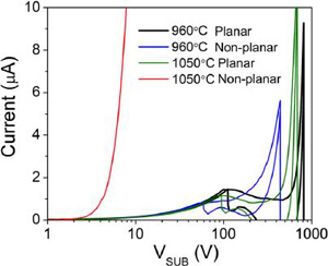 Figure 2: Breakdown voltage for planar and non-planar re-growth at p/n junction in n/p/n structure at two different p-GaN growth temperatures, 960°C and 1050°C.
The three-terminal breakdown was about 20V, caused by source-drain leakage that increased with drain bias. Tests with planar and non-planar pn GaN structures suggested that lowering the p-GaN re-growth temperature could improve breakdown characteristics (Figure 2).
The researchers comment: "This suggests a path to combine the high breakdown voltages demonstrated in planar n/p/n structures and transistors with low ON-resistance and high ON-current, enabling power transistors with higher power densities and higher average electric fields."
Planar structures with n/p/n layers achieved breakdown fields of 3.1MV/cm – close to the ~5MV/cm critical field value for bulk GaN.
Vertical GaN transistors CAVETs GaN MOCVD MBE
http://dx.doi.org/10.1063/1.4919866
The author Mike Cooke is a freelance technology journalist who has worked in the semiconductor and advanced technology sectors since 1997.


