


- News
13 May 2015
Room-temperature wafer bonding for multi-junction III-V solar cells
Researchers based in Japan and China have demonstrated a room-temperature wafer bonding technique to make multi-junction III-V solar cells [Masayuki Arimochi et al, Jpn. J. Appl. Phys., vol54, p056601, 2015]. The team from Sony Corp in Japan and the Chinese Academy of Sciences' Suzhou Institute of Nano-tech and Nano-bionics say that this is the first time that such methods have been used for solar cells consisting of aluminium gallium arsenide (AlGaAs) and indium gallium arsenide (InGaAs) absorbing layers.
The researchers comment: "To the best of our knowledge, the obtained GaAs || InGaAs and AlGaAs || InGaAs wafer-bonded solar cells exhibited the lowest ."
The team believes that wafer bonding can overcome the problems of lattice matching that occur when monolithic multi-junction devices are produced. However, wafer bonding techniques often require high-temperature annealing that can lead to wafer bending and void formation, along with dopant diffusion. These factors increase electrical resistance and create optical losses.
Room-temperature bonding has been developed for photovoltaic devices involving a combination of III-V materials with silicon, such as AlGaAs || Si, InGaP/GaAs || Si, and InGaP || Si. The researchers report: "Nevertheless, there have been no reports on room-temperature wafer-bonded solar cells that consist of only compound semiconductors, to the best of our knowledge."
The solar cell materials were grown using metal solid-source molecular beam epitaxy under ultra-high vacuum rather than metal-organic chemical vapor deposition (MOCVD) – avoiding residual impurities from organic precursors. The group III metals (Ga, Al, In) were supplied from effusion cells. The arsenic source was a valved cracking cell.
GaAs was used as a substrate for AlGaAs and GaAs solar cells. The In0.53Ga0.47As solar cell used a (001) InP substrate. The InGaAs solar cells were grown at 495°C. For the other devices, arsenide and phosphide layers were grown at 580°C and 510°C, respectively, apart from AlGaAs that was deposited at 710°C to improve quality. The lattice mismatch of all the structures was less than 10-4, according to x-ray analysis. Phosphides were used for window and back surface field (BSF) layers.
The InGaAs bottom-cell devices were wafer bonded at room temperature to either GaAs and AlGaAs cells (Figure 1). Before bonding, the back-side of the InGaAs cell was given p-ohmic contacts of gold/zinc/gold/chromium/gold by evaporation and annealing at 400°C for 3.5 minutes. The bonding surfaces were further prepared by planarization with chemical mechanical polishing (CMP).
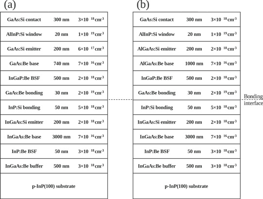
Figure 1: Schematics of (a) GaAs || InGaAs and (b) AlGaAs || InGaAs room-temperature wafer-bonded solar cell structures. Electrodes and etched contact layers are omitted.
During room-temperature bonding, the surfaces were irradiated with argon ions to create dangling bonds. The bonding force was 5000N. The n-ohmic contacts were formed after bonding with gold-germanium/nickel/gold fingers. The exposed GaAs surface was etched before RF sputtering of an anti-reflective coat of reflectivity ~3.5%. The devices were completed with 10 minutes of 350°C annealing of the n-contacts and dicing into 5mmx5mm chips.
Theoretical estimates of wafer-bonded AlGaAs || InGaAs solar cells suggested a peak efficiency of 33% for a structure with 11% aluminium-content AlGaAs. A GaAs || InGaAs solar cell would have 25% efficiency in the same calculation. The measured efficiencies fell short of these values (Table 1).
Table 1: Typical electrical properties of GaAs || InGaAs and AlGaAs || InGaAs room-temperature wafer-bonded solar cells along with single-junction solar cell properties under 1 sun AM1.5G spectrum. Shadow losses of bonded samples are 1% and 5%, respectively.
| Short-circuit current | Open-circuit voltage | Fill factor | Efficiency | |
| GaAs single-junction | 27.2mA/cm2 | 0.99V | 79.5% | 21.4% |
| InGaAs single-junction | 48.9mA/cm2 | 0.31V | 65.4% | 10.0% |
| GaAs || InGaAs wafer-bonded | 20.7mA/cm2 | 1.26V | 81.0% | 21.1% |
| AlGaAs single-junction | 22.7mA/cm2 | 1.05V | 79.7% | 19.0% |
| AlGaAs || InGaAs wafer-bonded | 21.4mA/cm2 | 1.32V | 77.8% | 22.1% |
In particular, the AlGaAs cell was found to have a lower open-circuit voltage 1.05V rather than the 1.11V expected from the GaAs cell voltage plus 0.12V for the difference in bandgap. The researchers suggest that "the quality of the AlGaAs single-junction solar cell was not sufficient, despite the high-temperature AlGaAs growth".
The voltage drop across the wafer bond was estimated at 0.04V, suggesting low electrical loss from this factor. The current mismatches between the cells adversely affected the short-circuit currents of the bonded devices, impacting efficiency benefits. The efficiency increased to 27.7% for an AlGaAs || InGaAS structure under 120-sun illumination (Figure 2).
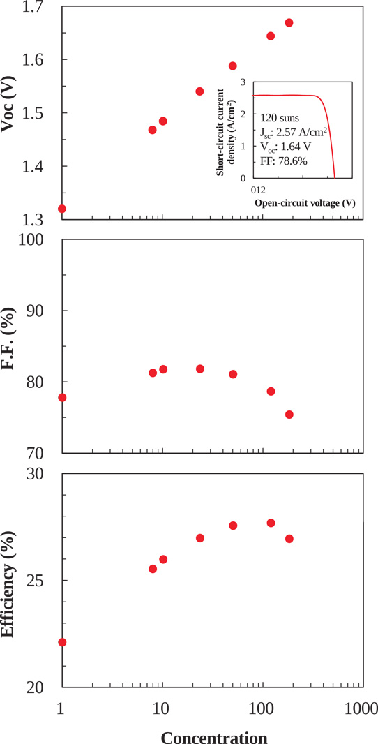
Figure 2: Solar cell properties of AlGaAs || InGaAs wafer-bonded solar cell as function of solar concentration ratio under AM1.5G spectrum. Inset: current-voltage characteristic at 120 suns.
The series resistance also increased under concentrated illumination to 4x10⁻²Ω-cm2 at 120 suns. Previous experiments with p+-GaAs/n-InP wafer bonding interfaces suggest that the resistance should be as low as 2.5x10⁻⁵Ω-cm2. The researchers believe that some of the problems at high concentration are due to the grid electrode being too thin (400nm) to handle the current generated.
Multi-junction III-V solar cells Room-temperature wafer bonding GaAs substrate AlGaAs InGaAs InP substrate MOCVD
http://dx.doi.org/10.7567/JJAP.54.056601
The author Mike Cooke is a freelance technology journalist who has worked in the semiconductor and advanced technology sectors since 1997.


