


- News
19 May 2015
Monolithic normally-off GaN switching devices with +5V threshold
Hongik University in South Korea has developed a normally-off monolithic gallium nitride (GaN) switching device on silicon, comprising a clamp circuit and normally-on metal-oxide-semiconductor heterostructure field-effect transistor (MOSHFET) [Sang-Woo Han et al, IEEE Electron Device Letters, published online 28 April 2015].
Normally-off devices are preferred for power switching applications in terms of low power consumption and fail-safe operation. Although normally-off GaN transistors have been produced using various techniques, the threshold voltages are only weakly positive and the on-current density is lower than for normally-on devices.
Hongik has integrated a Schottky barrier diode (SBD) and metal-insulator-metal (MIM) capacitor to create the clamp circuit that shifts the drive signal down to what is needed to switch the transistor on or off (Figure 1). The gate of the MOSHFET acts as a resistive load to the clamp.
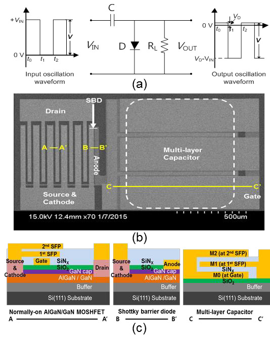
Figure 1: (a) Clamp circuit and input and output voltage waveforms, (b) SEM image of fabricated device, and (c) corresponding cross-sectional schematics.
The effect is to give an integrated device with normally-off operation, achieving a higher threshold voltage with high current density and low on-resistance than for normally-off GaN transistors.
Although Schottky diodes have been integrated before, the researchers believe that their structure is the first reported combination of a clamp circuit with a GaN FET.
The epitaxial material was grown on silicon (111) substrates with 3.9μm carbon-doped GaN buffer, 0.4μm GaN channel, 20nm Al0.25Ga0.75N barrier, and 2nm GaN cap.
Device fabrication began with mesa isolation from inductively coupled plasma (ICP) etching. The silicon dioxide (SiO2) gate insulator was grown using plasma-enhanced chemical vapor deposition (PECVD). The ohmic source/drain electrodes were silicon/titanium/aluminium/molybdenum/gold annealed at 800°C for 30 seconds in nitrogen.
Nickel/gold was evaporated to form the anode for the Schottky barrier diode, the MOSHFET gate, and the capacitor electrodes. The structure was annealed at 400°C for 20 minutes in oxygen. Finally, two source field-plates (SFPs) and multi-layer capacitor electrodes were fabricated using patterned nickel/gold and silicon nitride deposition.
The channel width of the MOSHFET was 5mm (10x500μm). The width of the SBD was 500μm. The capacitor rating was around ~800pF.
The prototype chip's capacitor is large in comparison with the MOSHFET. However, the researchers point out that the capacitor size would not need to be increased for larger MOSHFETs designed to handle higher currents. Normally-on GaN transistors also handle more current than similar size normally-off devices, reducing overall chip size.
Gate pinch-off occurred in the MOSHFET at -14V. The maximum drain current at 0V gate potential was 2.34A (~470mA/mm). The off-state breakdown was greater than 900V. The clamp circuit shifted the input range from 0V-20V to -19.2V-+0.8V at the gate.
When the SBD is forward biased (20V input, +0.8V gate), the current through it was ~1μA, "negligible compared to the FET on-current," according to the researchers.
In the off-state (0V input, -19.2V gate), the resistance between gate and source was ~200MΩ. The estimated time constant for capacitor discharge was ~160ms. The team says that this is long enough for stable switching operation.
The specific on-resistance at 1V drain bias was 19.4mΩ-cm2 according to the MOSHFET area. Including the clamp circuit increased this to 47.2mΩ-cm2. For larger MOSHFETs, one would expect this value to decrease towards the MOSHFET value, since the clamp circuit would be a smaller proportion of the chip.
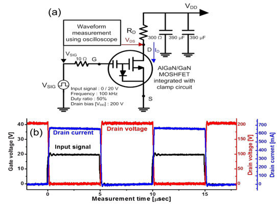
Figure 2: (a) Switching measurement setup and (b) demonstration of normally-off switching operation of AlGaN/GaN-on-Si MOSHFET with integrated clamp circuit.
The device was tested using a hard switching set up (Figure 2). The gate switching was performed at 100kHz with a 50% duty cycle. The virtual threshold of the MOSHFET and clamp was ~+5V (-14V - (-19.2V), pinch-off – clamp shift). This gives a higher effective threshold, compared with other techniques for creating normally-off GaN transistors (Table 1).
Table 1: Comparison of maximum current density, threshold voltage, and breakdown voltage with conventional normally-off GaN devices.
| Hongik device | P-type gate | Fluorine treatment | Recessed MIS | |
| Maximum current | 470mA/mm | 200mA/mm | 250mA/mm | 370mA/mm |
| Threshold | +5.2V (virtual) | +1V | +0.6V | +1.9V |
| Breakdown | 910V | 800V | 390V | 820V |
GaN switching device on silicon MOSHFET GaN FET GaN PECVD
http://ieeexplore.ieee.org/xpl/articleDetails.jsp?arnumber=7096943
The author Mike Cooke is a freelance technology journalist who has worked in the semiconductor and advanced technology sectors since 1997.


