


- News
25 March 2015
InGaN waveguides for increasing optical confinement in laser diodes
Researchers in Poland have been using indium gallium nitride (InGaN) waveguides to enhance optical confinement in 450nm-wavelength blue laser diodes (LDs), reducing threshold currents [Grzegorz Muziol et al, Appl. Phys. Express vol8, p032103, 2015]. The team from Institute of High Pressure Physics and TopGaN Ltd employed low-temperature plasma-assisted molecular beam epitaxy (PAMBE) in order to achieved high material quality with indium contents up to relatively high values of 8%.
The epitaxial material for the laser diodes was grown on c-plane bulk ammono-GaN substrates with a dislocation density of about 104/cm2. The layers up to and including the multiple quantum well (MQW) were constant in thickness with a 80nm InxGa1-xN bottom waveguide, and three 2.6nm In0.17Ga0.83N quantum wells separated by 8nm InxGa1-xN barriers.
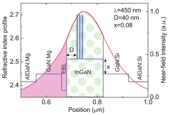
Figure 1: Refractive index profile and corresponding optical mode distribution of blue LD. Solid purple and dotted green regions correspond to optical mode confined within Mg-doped region and InGaN waveguide, respectively.
The emission wavelength of all devices was within 2nm of 450nm. The structure also included 700nm silicon-doped aluminium gallium nitride (Al0.065Ga0.935N) bottom cladding, designed to compensate for the tendency to bow caused by strain from the different lattice constants of GaN and InGaN. With the AlGaN bottom cladding the radius of curvature of the 1-inch substrate was in the range 40-60m.
The thickness D of the upper InxGa1-xN waveguide layer was varied up to 80nm. Increasing the indium content x up to 8%, and D to 80nm, reduced the laser threshold current (Figure 2). With D at 5nm and x at 8%, the threshold current was 12.5kA/cm2 – increasing D to 80nm reduced this to 3.6kA/cm2. Changing x from 4% to 8% reduced the threshold by 50%. Despite the increased distance between the electron-blocking layer (EBL) and MQW structure, the researchers found no decrease in injection efficiency.
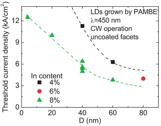
Figure 2: Threshold current density of LDs as a function of distance D between MQW and magnesium-doped EBL. Dashed lines are guides to the eye.
The researchers believe that the effect of increasing D is to reduce the overlap of the optical mode with the magnesium-doped layers of the device, which have larger optical absorption than undoped regions. However, increased x also increases optical absorption because the band-edge is closer to that of the quantum wells and also as a result of indium fluctuations in higher content material. At the same time, the refraction index contrast of high-x InGaN with the surrounding layers reduces optical leakage, enhances optical confinement, and increases differential gain of the light amplification.
http://dx.doi.org/10.7567/APEX.8.032103
The author Mike Cooke is a freelance technology journalist who has worked in the semiconductor and advanced technology sectors since 1997.


