


- News
5 March 2015
Skysilicon releases China's first GaN power transistor on 8-inch substrate
Skysilicon Co Ltd of Chong Qing City, China (which makes discrete power devices and power ICs, MEMS sensors and compound semiconductor devices) has released what is reckoned to be China's first gallium nitride (GaN) power device manufactured on an 8-inch substrate, specifically a GaN metal-insulator-semiconductor high-electron-mobility transistor (MISHEMT) fabricated on an 8-inch GaN-on-silicon wafer.
The firm says that, due to its performance, the N1BH60010A device can be used widely in power electronics systems, e.g. power factor correction (PFC), DC/DC converters, DC/AC inverters etc, in consumer, automotive and industrial markets.
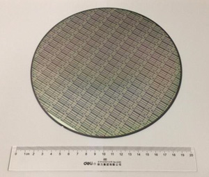 Picture: MISHEMT device fabricated on 8-inch GaN-on-Si wafer.
Compared with conventional semiconductor materials such as silicon and gallium-arsenide (GaAs), GaN features high breakdown electrical field, high saturation velocity, high power density and low intrinsic carrier density. Based on such performance, GaN devices can therefore be used for high-speed and high-efficiency power electronics applications. In addition, GaN-on-Si power devices have cost advantages, says Skysilicon. By increasing the diameter of the silicon substrate used for GaN epilayer growth, it is easy to reduce the unit device cost and achieve high-volume production, adds the firm. Skysilicon fabricated the GaN-on-Si power device platform on its in-house 8-inch manufactory line, which is capable of being used for high-volume production. GaN-on-Si has therefore been considered to be the most promising technology for next-generation power electronics applications.
Skysilicon began research on GaN-on-Si power devices in July 2013. After 18 months of development, it has developed a 600V/10A GaN MISHEMT on 8-inch silicon substrates that shows what are claimed to be good switching characteristics and small parasitic capacitance, i.e. ID > 10A, ID,pulse = 35A (pulse width = 600μs), VDSS = 600V, RDS(on) = 0.27Ω, IDSS < 10μA (VDS = 600V), IGSS < 10nA (VGS = -10V), CISS = 52pF, COSS = 26pF and CRSS = 21pF. Compared with a silicon super-junction MOSFET, the GaN MISHEMT can reduce parasitic capacitance by up to 90%, it is claimed. Also, reverse recovery charge can be eliminated due to the fact that there is no PN junction in the GaN device, indicating significant advantages for applications in high-efficiency and fast-switching power electronics systems. Compared to the major GaN power device suppliers, the main characteristics of Skysilicon's GaN power device are either comparable to or better regarding off-state leakage and parasitic capacitance, it is claimed.


