


- News
23 March 2015
Flip-chip packaging and gallium nitride power transistors
Researchers in Taiwan have been studying the effects of flip-chip packaging on the performance of gallium nitride (GaN) high-electron-mobility transistors (HEMTs) [Szu-Ping Tsai et al, Appl. Phys. Express, vol8, p034101, 2015]. Packaging three devices in parallel, the team from National Chiao-Tung University and Yuan Ze University found increased output current and reduced on-resistance, along with greater temperature insensibility. The researchers comment: "Superior performance such as this makes flip-chip packaging a potential technology for high-power GaN electronic applications."
GaN devices are being considered for replacements of silicon MOS parts for power supplies, inverters for electric vehicles (EV), photovoltaic (PV) inverters, and motor control for industry electronics. Flip-chip-packaged transistors with lower parasitic effects could also benefit radio-frequency applications.
The HEMT devices that were used had a 2μm gate length and 500μm gate width, realized using a 10-finger structure (Figure 1). The barrier material for the HEMT was aluminium gallium nitride (Al0.25Ga0.75N). The epitaxial structure – 120nm AlN buffer, 5.5μm GaN channel, 25nm AlGaN barrier, and 4nm GaN cap – was grown on a 650μm silicon substrate by metal-organic chemical vapor deposition (MOCVD).
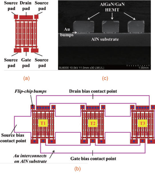
Figure 1: (a) Schematic layouts for single GaN transistor. (b) Schematic layouts for three GaN transistors flip-chip packaged in parallel. (Hollow purple outlines represent metal interconnects on substrate.) (c) SEM image of three GaN HEMTs flip-chip packaged in parallel.
The researchers screened the three devices to be packaged for similar key electrical characteristics, "to ensure that all the devices connected in parallel had balanced current sharing". AlN substrates were used as substrates for the flip-chip packaging process using gold-to-gold thermo-compression bonding at 250°C.
The saturation drain current with 0V gate potential was about 1A for the three devices. This allowed the parallel devices to achieve almost 3A when packaged. The on-resistance in the linear region was reduced to 1.3Ω, about one-third the value for the individual devices (4Ω).
Pulsed measurements with 0.02% duty cycle were performed to analyze thermal performance. Pulsed operation avoids self-heating effects. 'Calibration results' at various temperatures from measurements obtained with 0V gate and drain biases were compared with measurements with different quiescent drain bias voltages at 25°C to derive the respective channel temperatures.
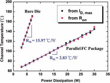 Figure 2: Estimated channel temperature as function of power dissipation.
The pulsed measurements allowed the researchers to estimate the thermal resistance of the bare dies and the packaged device (Figure 2). Packaging allowed the three transistors to operate at up to 30W power dissipation with a channel temperature restricted to less than 150°C. The bare dies reached 7W at 175°C.
The researchers comment: "This superior performance clearly indicates much better thermal management for applications of flip-chip technology in high-power electronics." The packaged devices also demonstrated lower thermal sensitivity. The thermal resistance was less than a fifth that of the bare dies.
http://dx.doi.org/10.7567/APEX.8.034101
The author Mike Cooke is a freelance technology journalist who has worked in the semiconductor and advanced technology sectors since 1997.


