


- News
18 March 2015
Direct growth of indium gallium nitride on silicon substrate
Researchers in Europe have developed a low-temperature plasma-assisted molecular beam epitaxy (PAMBE) process for direct growth of indium gallium nitride (InGaN) on silicon (Si) substrates [Pavel Aseev et al, Appl. Phys. Lett., vol106, p072102, 2015]. Silicon is an attractive substrate with a view to low-cost production and integration with silicon CMOS electronics.
GaN on silicon has been developed recently for high-power switching and high-frequency amplifier applications. Some work has also been performed on InGaN-based light-emitting devices using GaN templates on silicon. However, a direct growth on InGaN could open the way to a wider range of wavelengths and applications such as solar cells.
The low-temperature PAMBE deposition was able to produce InGaN layers across the range of compositions, including near-infrared, as used in 1.3μm and 1.55μm optical communications. The work was carried out at Universidad Politécnica de Madrid and Universidad de Cádiz in Spain, Max Planck Institute of Microstructure Physics and Carl von Ossietzky Universität Oldenburg in Germany, and Universitá di Milano-Bicocca in Italy.
The InGaN was grown on p-type silicon (111) substrates. Before deposition, the substrates were degassed at 850°C for 30 minutes and exposed to a nitrogen flux for 5 minutes to create a 2-3nm silicon nitride layer. Such nitridation has previously been found to improve strain relaxation and crystal quality for GaN growth on silicon.
The InGaN growth at 450°C lasted an hour. The growth temperature is low, even for MBE – GaN MBE is typically carried out at 700-800°C. The aim of the low temperature was to avoid indium desorption.
The growth conditions were slightly nitrogen-rich. The balance between the group-III metals (In, Ga) and nitrogen was important to avoid metallic droplet (metal-rich) or nanocolumn (nitrogen-rich) formation.
High-resolution transmission electron microscope (HRTEM) study of an In0.73Ga0.27N sample (Figure 1) showed "clear projections of atomic columns" apart from "occasional localized defects". High-angle annular dark-field (HAADF) imaging showed some slight variations in contrast from threading dislocations (TDs) or differences in sample thickness.
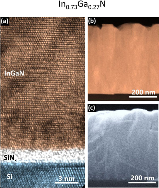
Figure 1: (a) HRTEM image of 480nm-thick In0.73Ga0.27N/SiNx/Si interface and (b) HAADF image of the InGaN layer, both taken along the [11–20] III-N zone axis. (c) Corresponding SEM image.
The researchers comment: "It is difficult to quantitatively deduce the density of the TDs as they are accumulated locally. Still, their density is lower or similar to that in other III-N layers grown on buffered silicon or sapphire substrates."
The team estimates the standard deviation for indium content at less than 2.5% on the basis of energy-dispersive X-ray (EDX) spectroscopy. The chemical homogeneity is attributed to the low growth temperature that suppresses compositional fluctuations and phase separation. One possible drawback of the low temperature was an undulating surface that is not seen with higher temperatures of more than 500°C.
The researchers point out that undulating surfaces can also be advantageous for many low-cost mass production applications "such as light-emitting diodes, solar cells, water splitting, and photodetectors".
Photoluminescence analysis at 10K of data from a near-field scanning optical microscope (NSOM) showed homogeneous peak intensity emission with ~15% standard deviation. The peak energy was around 1.24eV (near-infrared, 1μm wavelength). Intensity variation was attributed to differences in crystal quality rather than indium composition.
Samples with varying indium content were produced covering the whole range from GaN to InN. Photoluminescence intensity varied by a factor of four among the samples (Figure 2).
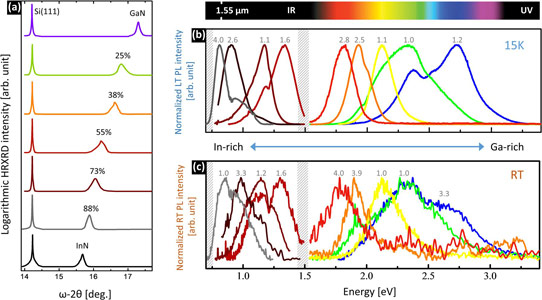
Figure 2: (a) High-resolution x-ray diffraction spectra recorded around symmetric InGaN(0002)/Si(111) Bragg reflection. Normalized photoluminescence spectra of InGaN layers taken at (b) 15K and (c) room temperature. Relative intensity scaling factors indicated. Low- and room-temperature intensities scale 95:1.
The electrical characteristics of the InGaN/p-Si junction were also measured. Above 50% indium content, the InGaN layer had an n-type majority carrier with defects acting as electron donors. This allowed an ohmic contact to be formed with titanium/aluminium/nickel/gold top contacts. The bottom contact was silver paste applied to the back-side of the silicon substrate.
The resulting structure gave 'near-ideal ohmic' current-voltage behavior for n-In0.53Ga0.47N/p-Si heterointerfaces, according to the researchers. Above 50% indium content, n-InGaN/p-Si junctions are expected to be ohmic due to alignment of the p-Si valence band and n-InGaN conduction band.
A structure with In0.37Ga0.63N/p-Si gave a rectifying behavior. The junction with the top metal contact was found to be still ohmic, but more resistive, due to the lower n-type carrier density.
PAMBE GaN InN InGaN Silicon substrate
http://dx.doi.org/10.1063/1.4909515
The author Mike Cooke is a freelance technology journalist who has worked in the semiconductor and advanced technology sectors since 1997.


