


- News
19 March 2015
IBM attaches silicon photonic chips directly onto processor package
The computing and telecoms industries are developing systems to store information in the cloud and analyze enormous amounts of data. IBM Research says that it has demonstrated what could be a key step toward commercializing this next generation of computing technology by establishing a method to integrate silicon photonic chips with the processor in the same package, avoiding the need for transceiver assemblies. "This integration scheme has the potential to massively reduce the cost of applying silicon photonics optical interconnects in computing systems"
The new technique, being presented on 25 March at the Optical Fiber Communication conference & exposition (OFC 2015) in Los Angeles, CA, USA (Presentation W3A.4, 'Silicon Photonics for the Data Center'), should be able to lower the cost and increase the performance, energy efficiency and size of future data centers, supercomputers and cloud systems.
Compared with traditional electronic links in existing computers, optical links using photonic devices can transmit more information over larger distances and are more energy efficient than copper-based links. To optimally benefit from this technology, a tight integration of the electrical logic and optical transmission functions is required. The optical chip needs to be as close to the electrical chip as possible to minimize the length of electrical connection between them. This can only be accomplished if they are packaged together, says IBM.
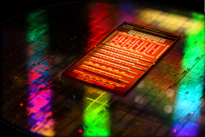 Picture: A CMOS silicon photonics chip.
"IBM has been a pioneer in the area of CMOS-integrated silicon photonics for more than 12 years," claims Bert Offrein, manager of the photonics group at IBM Research - Zurich. "In addition to the silicon technology advancements at the chip-level, novel system-level integration concepts are also required to fully profit from the new capabilities silicon photonics will bring," he adds.
Optical interconnect technology is currently incorporated into data centers by attaching discrete transceivers or active optical cables (AOCs), which come in pre-assembled building blocks. The pre-packaged transceivers are large and expensive, limiting their large-scale use, Offrein says. Furthermore, such transceivers are mounted at the edge of the board, resulting in a large distance between the processor chip and the optical components.
Offrein and his IBM colleagues from Europe, the USA and Japan instead proposed an integration scheme in which the silicon photonic chips are treated similarly to ordinary silicon processor chips and are directly attached to the processor package without pre-assembling them into standard transceiver housings. This improves the performance and power efficiency of the optical interconnects while reducing the cost of assembly. Challenges arise because alignment tolerances in photonics are critical (sub-micron range) and optical interfaces are sensitive to debris and imperfections, requiring the best in packaging technology.
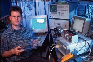 Picture: Bert Offrein, manager of the photonics group at IBM Research – Zurich, holds an example of silicon photonic chips integrated with an array of polymer waveguides.
The team demonstrated efficient optical coupling of an array of silicon waveguides to a substrate containing an array of polymer waveguides. The significant size difference between the silicon waveguides and the polymer waveguides originally presented a major challenge, says IBM. The researchers overcame this obstacle by gradually tapering the silicon waveguide, leading to efficient transfer of the optical signal to the polymer waveguide.
The method is scalable and enables the simultaneous interfacing of many optical connections between a silicon photonic chip and the system. The optical coupling is also wavelength and polarization insensitive and tolerant to alignment offsets of a few microns, Offrein says.
"This integration scheme has the potential to massively reduce the cost of applying silicon photonics optical interconnects in computing systems," Offrein reckons. Cheaper photonic technology enables its deployment at a large scale, which could lead to computing systems that can process more information at higher performance levels and with better energy efficiency, he adds.
"Such systems will be key for future applications in the field of cloud-computing, big data, analytics and cognitive computing," Offrein continues. "In addition, it will enable novel architectures requiring high communication bandwidth, as for example in disaggregated systems."
IBM announces $3bn research initiative to tackle chip challenges for cloud and big-data systems
www.research.ibm.com/photonics


