


- News
17 June 2015
Vertical Schottky barrier diodes on free-standing n-type aluminium nitride
Researchers based in Japan and USA have reported the fabrication of vertical Schottky barrier diodes (SBDs) on aluminium nitride (AlN) substrates for the first time [Toru Kinoshita et al, Appl. Phys. Express, vol8, p061003, 2015]. The team involved researchers from Tokuyama Corp, Fuji Electric Co Ltd and Tokyo University of Agriculture and Technology in Japan, along with HexaTech Inc and North Carolina State University in the USA.
AlN has an extremely wide 6.1eV bandgap: The wider the bandgap, the higher the expected breakdown voltages, opening up power electronics applications. AlN also has a high thermal conductivity of 3.2W/cm-K, enabling higher power density. The wide bandgap is also attractive for deep ultraviolet (~200nm) light emission.
One barrier to AlN power electronics is developing n-type conductivity in thick layers so that free-standing substrates can be developed. Metal-organic chemical vapor deposition (MOCVD) is slow (~1μm/hour). Hydride vapor phase epitaxy (HVPE) is much faster and enables such a development.
The silicon-doped AlN HVPE was carried out at 1450°C on 15mm-diameter highly insulating 10TΩ-cm AlN substrates. The growth substrates were produced in a physical vapor transport (PVT) process at HexaTech. The Al-polar growth surface was prepared using chemical mechanical polishing (CMP. The average HVPE growth rate was 25μm/hour.
X-ray analysis showed that the crystal quality of the HVPE material was similar to that of the PVT substrate. Secondary-ion mass spectrometry (SIMS) gave uniform values for impurity concentrations of silicon, oxygen, and carbon. The silicon concentration of the AlN:Si was 3x10¹⁷/cm3.
Hall measurements on a 32μm AlN:Si layer resulted in 2.4x10¹⁴/cm3 net electron concentration, 115cm2/V-s mobility, and 2.3x10²Ω-cm resistivity. The concentration was the same order as for AlN:Si grown using MOCVD. However, the HVPE mobility was lower than for MOCVD. At the same time, the HVPE dislocation density is estimated to be at least four orders of magnitude lower than for MOCVD. The researchers attribute the counter-intuitive mobility result as being due to a higher number of point defects in the HVPE material.
Temperature-dependent Hall analysis gave a donor density of 2.6x10¹⁷/cm3, an acceptor density of 1.5x10¹⁷/cm3, and a donor activation energy of 245meV. The activation energy was similar to values reported for MOCVD AlN. "These results revealed that HVPE can produce AlN:Si layers with n-type conductivity similar to those grown by MOCVD," the researchers write.
Schottky barrier diodes (Figure 1) were fabricated from a 250μm-thick AlN layer, which was subjected to chemical mechanical polishing on the AlN:Si side and mechanical polishing to remove the PVT AlN substrate. The resulting free-standing AlN:Si was 150μm thick.
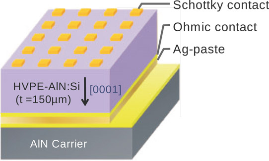
Figure 1: Schematic vertical Schottky barrier diode on HVPE-AlN:Si substrate.
Annealed titanium/aluminium/titanium/gold on the Al-polar surface was used as the ohmic contact. Several 270μmx270μm Schottky nickel/gold contact electrodes were applied to the N-polar side. The device was mounted ohmic side down on a ceramic AlN carrier with silver paste.
The turn-on voltage was 2.2V. The series resistance was 3.5x10⁶Ω, much higher than the value expected from the Hall mobility. The researchers suggest that this could be due to high resistance damage from mechanical polishing of the surface on which the Schottky contacts are made. Increasing the temperature to 373K reduced the series resistance to 2.9x10⁵Ω.
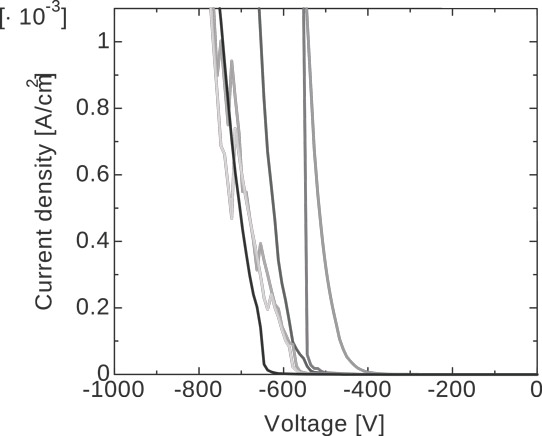
Figure 2: Reverse current–voltage characteristics of vertical Schottky barrier diodes on free-standing n-type HVPE-AlN substrate.
Reverse-bias leakage was less than 10-6A/cm2 below 400V. Reverse breakdown voltages for 10-3A/cm2 were between 550V and 770V for six devices. Since the thermionic field emission theory breakdown voltage for the device was 200V, the researchers believe that the ionized donor concentration is significantly lower than the silicon concentration. Toru Kinoshita of Tokuyama reports that a mid-1016/cm3 value for the ionized donor concentration would fit the 550–770V breakdown behavior.
The researchers comment that the large discrepancy between experimental and theoretical breakdown values might be reduced by suppressing the effect of surface damage and by creating better defined Schottky contacts.
Vertical Schottky barrier diodes Free standing n-type aluminium nitride AlN substrates HVPE
http://dx.doi.org/10.7567/APEX.8.061003
The author Mike Cooke is a freelance technology journalist who has worked in the semiconductor and advanced technology sectors since 1997.


