


- News
3 June 2015
Improving gallium nitride LED material quality using carbon nanotubes
Researchers in China have used carbon nanotube (CNT) layers to improve the material quality and performance of indium gallium nitride (InGaN) light-emitting diodes (LEDs) [Liang Shan et al, Jpn. J. Appl. Phys., vol54, p065102, 2015].
Yantai University, Chinese Academy of Sciences' Institute of Semiconductors, and Tsinghua University used the CNTs to create patterned sapphire substrates (CNPSS) on which to grow III-nitride epitaxial layers. The aim was to improve both crystal quality and light extraction efficiency. Threading dislocations (TDs) reduce the efficiency of light emission from III-nitride devices. Further, a large difference in refractive index between GaN and air causes many of the emitted photons to be reflected back and trapped in LED devices.
The CNT layers were designed to improve crystal quality in a manner similar to epitaxial lateral overgrowth, where a mask restricts the nucleation of the GaN growth to a few small areas. The crystal then grows from these seed areas and coalesces to form material with fewer threading dislocations.
The CNTs were grown on 4-inch silicon substrates using low-pressure chemical vapor deposition (CVD) using a 5nm iron film as catalyst. The precursor was acetylene (C2H2). The CNTs were formed in superaligned arrays with diameters of ~15nm. The aligned film was dry spun from the silicon substrate and transferred to 2-inch c-plane sapphire wafers. A focused laser beam was used to align the CNTs with particular directions of the subsequent GaN crystal structure. In multi-layer structures, the directions of the CNTs in successive layers were perpendicular.
The wafer was dipped in ethanol and dried. The CNTs bunched together in 2-4μm bundles. The gaps between the bundles were 200-500nm.
The LED heterostructure was grown using metal-organic chemical vapor deposition (MOCVD): 30nm GaN buffer, a recovery layer, 3.5μm undoped GaN, 2.3μm n-GaN, InGaN/GaN multiple quantum well (MQW), p-AlGaN/p-GaN superlattice, and 80nm p-GaN. The MQW consisted of a 9-period structure with 3nm wells and 10nm n-type barriers.
The LED chips consisted of 45milx45mil (1.14mmx1.14mm) mesas surrounded by an exposed n-GaN contact. The p-GaN was covered in nickel/silver/platinum/gold serving as reflector and contact. The n-contact was chromium/platinum/gold. The resulting chips were bonded to silicon submounts.
Table 1: Full-width at half maximum (FWHM) values for (002) and (102) rocking-curve peaks, estimated dislocation densities. Results for CNPSS structures up to three CNT layers and conventional sapphire substrate (CSS) are compared.
| Sample | (002) FWHM | (102) FWHM | Screw-type | Edge-type |
| CNPSSI-LED | 290.6arcsec | 405arcsec | 1.70x10⁸/cm2 | 60.49x10⁸/cm2 |
| CNPSSII-LED | 284.4arcsec | 402.8arcsec | 1.63x10⁸/cm2 | 60.56x10⁸/cm2 |
| CNPSSIII-LED | 261.2arcsec | 384.9arcsec | 1.37x10⁸/cm2 | 56.81x10⁸/cm2 |
| CSS-LED | 275.6arcsec | 489.9arcsec | 1.52x10⁸/cm2 | 101.38x10⁸/cm2 |
X-ray analysis of GaN epitaxial material grown on CNT-patterned sapphire substrates (CNPSS) was used to assess the density of screw- and edge-type dislocations (Table 1). The decreasing density of threading dislocations with number of CNT layers (I-III) was attributed to the narrower windows between CNT bundles in which the GaN can nucleate. "These reduced nanoscale windows can result in faster and more uniform coalescence of neighboring nano-islands, which can further reduce the TD density in the overgrown GaN films because of reduced strain and misorientation between these nano-islands," the researchers comment.
Table 2: Current leakage at 10V reverse bias, light output power at 350mA injection, transmittance of 450nm wavelength light of CNT layers relative to CSS, and divergence angle of output radiation at 350mA.
| Sample | Leakage | LOP | Relative transmittance | Half-maximum divergence |
| CNPSSI-LED | 1.21μA | 213.8mW | 75% | 145° |
| CNPSSII-LED | 0.77μA | 262.4mW | 70% | 144° |
| CNPSSIII-LED | 0.35μA | 266.3mW | 50% | 142° |
| CSS-LED | 2.74μA | 194.2mW | 100% | 158° |
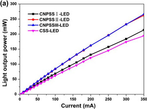 Figure 1: Light output power for LEDs.
The improved crystal structure results in reduced leakage current at a reverse bias of 10V (Table 2). The forward voltage at 350mA injection current was ~3.62V for all devices, including the conventional sapphire substrate (CSS) version.
The light output power (LOP) increased with the number of CNT layers (Figure 1, Table 2). The main improvement came from the reduction of dislocation density in the LED epitaxial material. "Additionally, photons had more opportunities to be extracted to the outside, owing to the diffraction of CNTs," the researchers write.
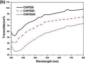 Figure 2: Transmittance of CNPSS based on baseline of transmittance of CSS.
The similarity of the LOP for two and three layers of CNT is attributed to increased absorption as the number of layers increases (Figure 2, Table 2). The angular dispersion of the radiation with CNTs is also directed more into the forward direction, reducing losses of optical power from photon trapping by internal reflection at interfaces of different refractive index. "The CNPSS-LED has suppressed lateral guiding modes and the trapped photons are re-directed into radiated modes," the researchers explain.
Carbon nanotubes LEDs GaN InGaN Sapphire substrates MOCVD
http://dx.doi.org/10.7567/JJAP.54.065102
The author Mike Cooke is a freelance technology journalist who has worked in the semiconductor and advanced technology sectors since 1997.


