


- News
2 July 2015
Neutral pH electrochemical etching of silicon-doped gallium nitride
Yale University in the USA has developed an electrochemical process of porous structures in gallium nitride (GaN) involving neutral pH solutions of common salt (NaCl) or sodium nitrate (NaNO3) [Mark J. Schwab et al, Appl. Phys. Lett., vol106, p241603, 2015]. The researchers comment: "These results open up the possibility of using safe and environmentally friendly etchants for processing GaN films, along with demonstrating crystallographic alignment of pores in anodically etched GaN."
Normally, wet etching of GaN involves acidic or basic solutions that are often extremely toxic. Porous etching could be used in chemical sensor applications.
The researchers developed their etching techniques using GaN templates grown on c-plane sapphire via metal-organic chemical vapor deposition (MOCVD). The GaN layers consisted of an unintentionally doped buffer and 2μm of silicon-doped n-type material. The wafers were diced into 1.5cmx0.5cm chips.
The electrochemical etching solutions were 0.3M NaNO3 or 3M NaCl. A 0.3M nitric acid (HNO3) solution was also used for comparison with NaNO3 etching. The NaNO3 and HNO3 solutions were used to etch layers with 3x10¹⁸/cm3 doping density. The NaCl was used on more heavily (2x10¹⁹/cm3) doped GaN.
The GaN was electrically connected through a metallic tape electrode. The counter-electrode was a platinum wire cathode. The bias was applied before the samples were lowered at 1cm/minute into the etching solution. The aim of the 45 second dipping stage was uniform etching of the sample. Including the dipping, the sample etch lasted for 2 minutes. An exception was an NaCl etch carried out for 30 minutes with low 6V bias. The etch time was sufficient to fully etch the doped layer, after which the current dropped to near zero.
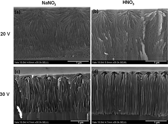
Figure 1: Angled cross-section views of films etched at (a) 20V in NaNO3, (b) 20V in HNO3, (c) 30V in NaNO3, and (d) 30V in HNO3. The films etched at 20V show highly branching pores, while films etched at 30V display vertically aligned pores beneath nucleation layer.
The etched material consisted of a low-porosity top 'nucleation layer' near the top surface from which the pores branch out (Figure 1). The researchers comment: "This nucleation layer is left largely intact because etching accelerates in the vicinity of the initial etch pits due to the enhancement of the electric field from the radius of curvature."
The density of pore mouths for NaNO3 was significantly lower than for HNO3 etching (Table 1). However, the pore density deep within the GaN was about the same for these etchants. Other etching characteristics were also largely similar for NaNO3 and HNO3 etching.
Table 1: Density of pore mouths at various etch conditions.
| NaNO3 | HNO3 | |
| 20V | 3.6x107cm2 | 1.1x108cm2 |
| 30V | 4.2 x108cm2 | 5.5x108cm2 |
Although previous reports of chemical etching suggested the gallium product was Ga2O3, this is not soluble in a neutral pH context. The researchers suggest a different reaction product – Ga(NO3)3, which is soluble.
The NaCl etch was preferential along certain crystallographic directions at the low bias of 6V, unlike the NaNO3 etch, which proceeds in the direction of the current (Figure 2). The researchers explain: "The walls of these triangular pores are oriented at 58° to the (0001) plane, which indicates that the {10–1-1} family of planes is resistant to etching in NaCl. The {10–1-1} planes are polar and have previously been noted to act as etch-terminating planes in photo-chemical etching of GaN, photo-electro-chemical etching, and hot-wet chemical etching."
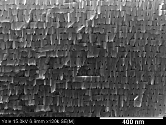
Figure 2: Film etched in NaCl at 3M concentration at 6V with 2 x10¹⁹/cm3 doping density. Triangular pores are bounded by {10-1-1} and (0001) planes.
Even at higher biases, the NaCl etch has a crystallographic preference. The researchers suggest that the chlorine atoms passivate {10-1-1} facets, inhibiting further etch in that direction.
The neutral pH etch could be extended in various ways, such as employing the technique on layers with different doping levels or using a low ~3V bias in combination with ultraviolet illumination. The latter photo-electro-chemical etching could also be combined with photoresist masking for selective processes.
The researchers report: "It has also been shown that selective etching is possible by growing GaN films with different layered doping levels, and using conductivity-selective etching to etch away highly doped layers while leaving the low-doped layers intact, giving the ability to create devices such as cantilevers and distributed Bragg reflectors."
Etching of silicon-doped gallium nitride Etch GaN MOCVD Sapphire substrates
http://dx.doi.org/10.1063/1.4922702
The author Mike Cooke is a freelance technology journalist who has worked in the semiconductor and advanced technology sectors since 1997.


