


- News
15 July 2015
Transparent conductive oxides and wafer bonding of III-Vs and silicon
The National Renewable Energy Laboratory (NREL) and University of California Santa Barbara in the USA have developed a wafer bonding technology for III-V materials and silicon (Si) using transparent conductive oxide (TCO) interlayers of indium zinc oxide (IZO) [Adele C. Tamboli et al, Appl. Phys. Lett., vol06, p263904, 2015]. The plasma-activated bonding is carried out at low temperature (200°C), avoiding thermal expansion mismatch problems. TCO interlayers protect the semiconductor from oxidation during the plasma activation.
The researchers see the process being used to create tandem solar cells with GaInP top cells and (amorphous/crystalline) heterojunction with intrinsic thin layer (HIT) silicon bottom cells. HIT-type cells already incorporate transparent conductive oxide as the top surface. "Such a device is promising for >30% efficiency 1-sun or low concentration solar cells at reasonable costs," the researchers write.
Apart from photovoltaic applications, the technique could also find use in integrating III-V optoelectronics with Si CMOS electronics. The researchers believe the process could also be used with other TCO materials such as indium tin oxide (ITO).
Two test samples of wafer-bonded materials were produced (Figure 1): III-V-to-sapphire and III-V-to-Si. The first sample was for optical characterization and the second for electrical testing. The sapphire was 430μm-thick double-side-polished c-plane crystal. The heavily n-type Si substrate was 500μm thick with 0.001-0.005Ω-cm resistivity.
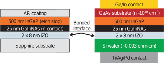
Figure 1: Schematics of test structures used to demonstrate TCO-based wafer bonding: structure on left used to measure optical properties; (b) structure on right used for testing electrical properties.
The III-V material consisted of heavily n-type (100) gallium arsenide (GaAs) substrate, 500nm n-type gallium indium phosphide (Ga0.5In0.5P) etch stop, and 25nm heavily n-type gallium indium nitride arsenide (GaInNAs) contact. The GaInNAs was doped with selenium.
The 8nm amorphous indium zinc oxide (IZO) wafer-bonding surfaces were created with RF sputtering. The IZO layer thickness was kept thin to avoid parasitic reflectance – the estimated reflection from the layer for GaInP/IZO/Si was 3.2% at 700nm wavelength, just below the GaInP band edge, and 1.0% at 1200nm, near the silicon band edge.
The III-V material was separated into 1cmx1.2cm pieces. Before bonding, the samples were cleaned in acetone, isopropanol and tergitol. The 30-second 100W oxygen plasma activation was carried out in an EVG 810 tool. After activation, the samples were stacked face-to-face and bonded in 225mbar vacuum, using a Süss SB6 system.
For the optical testing, the GaAs substrate was etched away in a 1:1 mix of hydrogen peroxide and ammonium hydroxide. A wax coating was used to avoid parasitic etching of the IZO and GaInNAs layers. An anti-reflection coat was added to the exposed GaInP consisting of 75nm magnesium fluoride and 40nm zinc sulfide. The III-V/Si sample was prepared for electrical testing by adding contacts.
For bonding, the IZO surfaces need to be flat and atomic force microscopy (AFM) measurements gave roughness estimates of less than 0.1nm root mean square.
A range of bonding temperatures up to 400°C were tested. High-temperature bonding resulted in cracking due to thermal expansion mismatches. At the medium temperature of 200°C, the III-V/Si sample bonded over large areas with an adhesion strength of 0.3MPa.
The researchers comment: "This bond strength is lower than optimized Si-Si plasma-activated bonds (11MPa), since the high temperatures necessary to convert hydrophilic to covalent bonds must be avoided due to thermal expansion mismatch."
Reducing the bonding temperature to 100°C decreased the bond strength, "presumably due to large unbonded areas, which were visible as interference fringes at the III-V/sapphire samples," the researchers add.
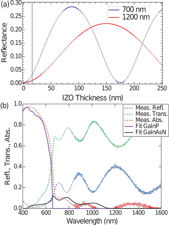
Figure 2: (a) Calculated reflectance of IZO layers of varying thickness sandwiched between GaInP and Si. (b) Measured optical properties of III-V/IZO/sapphire bonded samples.
In the light absorption tests (Figure 2), the majority of the less than 10% of parasitic loss occurred in the n-GaInNAs contact layer with 1eV bandgap. This layer is needed for ohmic contact between the IZO and GaInP. The GaInNAs could be thinned or replaced with a more optimized material, the researchers believe.
The optimal electrical resistance of less than 0.5Ω-cm2 was achieved with 200°C bonding. At higher temperatures, cracking inhibited current spreading; at low temperatures, the current flow was restricted by the reduced bonding area. The researchers comment: "These results would contribute a voltage loss of <10mV in a tandem cell operating at 1 sun (20mA/cm2), sufficient for a high-efficiency tandem cell."
TCO IZO Tandem solar cells GaInP Silicon GaAs substrates
http://dx.doi.org/10.1063/1.4923444
The author Mike Cooke is a freelance technology journalist who has worked in the semiconductor and advanced technology sectors since 1997.


