


- News
15 July 2015
Leti and EVG launch INSPIRE nano-imprint lithography program
Micro/nanotechnology R&D center CEA-Leti of Grenoble, France and EV Group of St Florian, Austria (a supplier of wafer bonding and lithography equipment for MEMS, nanotechnology and semiconductor applications) have launched a program in nano-imprint lithography (NIL) called INSPIRE to demonstrate the benefits of versatile nano-patterning technology and spread its use for applications beyond semiconductors.
In addition to creating an industrial partnership to develop NIL process solutions, INSPIRE aims to demonstrate the technology's cost-of-ownership benefits for a wide range of application domains, such as photonics, plasmonics, lighting, photovoltaics, wafer-level optics and bio-technology.
Leti and EVG will jointly support the development of new applications from the feasibility-study stage to supporting the first manufacturing steps on EVG platforms and transferring integrated process solutions to their industrial partners, thus significantly lowering the entry barrier for adoption of NIL for manufacturing novel products.
In its effort to support high-volume manufacturing applications, in early July EVG launched the HERCULES NIL equipment platform, and the INSPIRE program's activities will complement the firm's efforts within the framework of its NILPhotonics Competence Center (launched in December 2014).
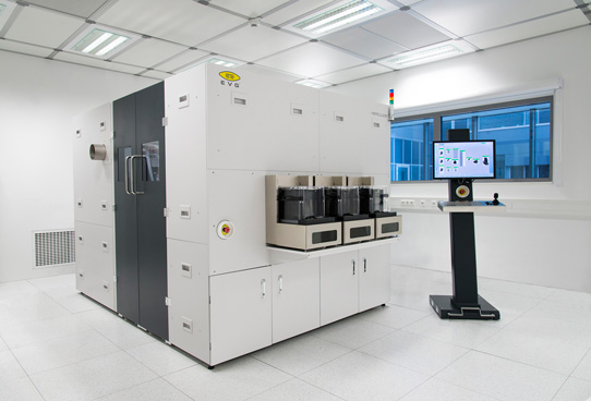
Picture: EVG's Hercules NIL system.
"After more than a decade of R&D activities, EVG has propelled NIL technology to a level of maturity that enables significant advantages for certain applications compared to traditional optical lithography," claims EVG's corporate technology development & IP director Markus Wimplinger.
After launching its NIL technology-development program more than 10 years ago, Leti oriented the use of the technology mainly for photonics applications. In early 2014, the program was integrated in the Silicon Technologies Division to establish a NIL collaborative program.
"Leti and EVG have a long history of collaborating on ways to bring new technologies to market at reasonable costs for the benefits of our customers," notes Laurent Pain, patterning program manager in Leti's Silicon Technologies Division. "Through INSPIRE, we will develop new ways for them to use this flexible, powerful nano-patterning technology to create new products for a wide range of applications."
EVG ramps nanoimprint lithography into high-volume manufacturing with HERCULES NIL track system
EV Group's NILPhotonics Competence Center generates strong interest
EVG establishes NILPhotonics Competence Center
www.evgroup.com/en/products/lithography/nanoimprint_systems


