


- News
7 July 2015
EVG ramps nanoimprint lithography into high-volume manufacturing with HERCULES NIL track system
EV Group of St Florian, Austria (a supplier of wafer bonding and lithography equipment for MEMS, nanotechnology and semiconductor applications) has unveiled the HERCULES NIL — a fully integrated track system that combines cleaning, resist coating and baking pre-processing steps with EVG's proprietary SmartNIL large-area nanoimprint lithography (NIL) process in a single platform.
Offering what is claimed to be industry-leading productivity and throughput, the system provides a complete, dedicated UV-NIL solution suited to high-volume manufacturing (HVM) of emerging photonic devices. It does so by imprinting structures in sizes ranging from tens of nanometers up to several microns that alter or improve the optical response of surfaces and devices, such as anti-reflective layers, color and polarizer filters, light-guiding plates, and patterned sapphire substrates (PSS) used in manufacturing light-emitting diodes (LEDs). Other rapidly emerging applications for NIL include MEMS (micro-electro-mechanical systems), NEMS (nano-electro-mechanical systems), biological and nano-electronic applications.
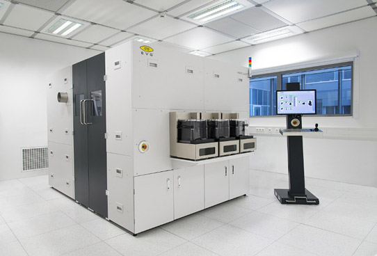
Picture: EVG's HERCULES NIL track system.
"After more than a decade of research and continuous improvements, EVG has now propelled NIL technology to a level of maturity that enables significant advantages for certain applications compared to traditional optical lithography," says executive technology director Paul Lindner. "In addition, the Hercules NIL allows a wider array of applications, particularly in the fields of photonics and biotechnology, to finally leverage the cost-of-ownership and resolution benefits of NIL in volume production," he adds.
The Hercules NIL combines EVG's expertise in nanoimprint lithography, resist processing and high-volume manufacturing solutions into a single integrated system that offers throughput of 40wph (wafers per hour) for 200mm wafers. The system is built on a highly configurable and modular platform that accommodates a variety of imprint materials and structure sizes — giving users greater flexibility in addressing their manufacturing needs. The fully integrated approach also minimizes the risk of particle contamination.
Key attributes include:
- fully automated UV-NIL imprinting and low-force detachment;
- full-area imprint coverage (avoiding pattern stitching errors associated with step-and-repeat lithography systems due to limited field size);
- volume manufacturing of structures down to 40nm and smaller;
- highest coating uniformity of +/-1% (resulting in minimal residual layer thickness and variation for processed structures over the entire wafer);
- supports a wide range of structure sizes and shapes (including 3D);
- ability to be used on high-topography (rough) surfaces; and
- ability to fabricate multiple-use soft stamps to extend the lifetime of master imprint templates.
Available now, HERCULES NIL systems have already been installed and are being used for high-volume manufacturing at production sites of leading photonic device manufacturers, says EVG.
EV Group's NILPhotonics Competence Center generates strong interest
EVG establishes NILPhotonics Competence Center
www.evgroup.com/en/products/lithography/nanoimprint_systems


