


- News
5 January 2015
High-temperature and concentrated PV performance of GaInN wells
Rensselaer Polytechnic Institute in the USA has developed nitride semiconductor solar cells with high quantum efficiency for short wavelengths (370-450nm) and concentrated photovoltaics at temperatures up to 400°C [Liang Zhao et al, Appl. Phys. Lett., vol105, p243903, 2014].
The researchers see the cells as being potential ‘top cells’ of multi-junction and hybrid devices. Although the bulk of solar radiation intensity occurs at shorter wavelengths, the absorption of the higher-energy shorter wavelengths can be a significant source of heating, raising solar cell temperatures and degrading performance.
The solar cells structures were grown on c-plane sapphire using metal-organic vapor phase epitaxy. The active region consisted of 2.5nm multiple quantum wells (MQWs) of gallium indium nitride (GaInN) separated by 20nm gallium nitride barriers. The wells contained an 8% molar fraction of InN. The MQWs were grown on 2μm n-GaN on the substrate. The p-type top layers consisted of 20nm aluminium gallium nitide (AlGaN) and finally 200nm GaN.
The cell fabrication consisted of etching 350μmx350μm mesas and depositing semi-transparent nickel/gold as the p-contact and titanium/aluminium/titanium/gold for the n-contact. The researchers report that they did not make any special effort to improve the light coupling into the devices.
Table 1: Short-circuit current density (JSC) and open-circuit voltage (VOC) under 1-sun AM1.5 illumination.
| QWs | JSC | VOC |
| 8 | 0.26mA/cm2 | 2.12V |
| 25 | 0.51mA/cm2 | 2.07V |
| 40 | 1.35mA/cm2 | 0.86V |
Devices with 8, 25 and 40 quantum wells were produced. In testing under AM1.5G solar simulated radiation (Table 1), the 40-QW device showed degraded performance in terms of open-circuit voltage (VOC) and leakage current. This was attributed to V-defects that began to appear when more than 20 quantum wells were grown.
The researchers believe that this problem could be resolved in future development aimed at controlling and avoiding V-defect formation. The hopeful result of such development would be JSC more than 1mA/cm2 with VOC more than 2V. In fact, the team believes that 40 wells are needed for ‘full absorption’ of the short-wavelength (370-450nm) radiation.
Estimates of the internal quantum efficiency (IQE) gave a 94% peak at 434nm for the 8-well structure. The 25-well cell showed a broader plateau of ~70% in the narrow 370-450nm range. Internal power conversion efficiency was put at 42.0% for the 8-well and 38.6% for the 25-well structures.
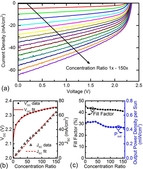
Figure 1: (a) Current-voltage behavior of 25-well cell passively cooled on aluminium chuck under concentrated illumination up to 150 suns. (b) VOC and JSC as functions of concentration ratio. (c) Fill factor and output power density per sun as functions of concentration ratio.
The 25-well cell was also subjected to concentrated AM1.5G illumination up to 150 suns (Figure 1). The ratio of maximum output power to the product of JSC and VOC – the ‘fill factor’ – decreased slightly from 45% to 41% as the number of suns increased. The maximum output power density per sun initially peaked at 0.51mW/cm2 for 40-sun illumination. The values at 1-sun and 150-suns were 0.49mW/cm2 and 0.42mW/cm2, respectively.
The researchers comment: “With a value above 0.4mW/cm2 and an overall loss of not more than 14% for the partial spectrum performance (350-450nm) up to concentrations of 150 suns without any active cooling, these results demonstrate the strong potential of the material system as an actively collecting junction and spectral filter for a lower thermal load in secondary conventional solar junctions.”
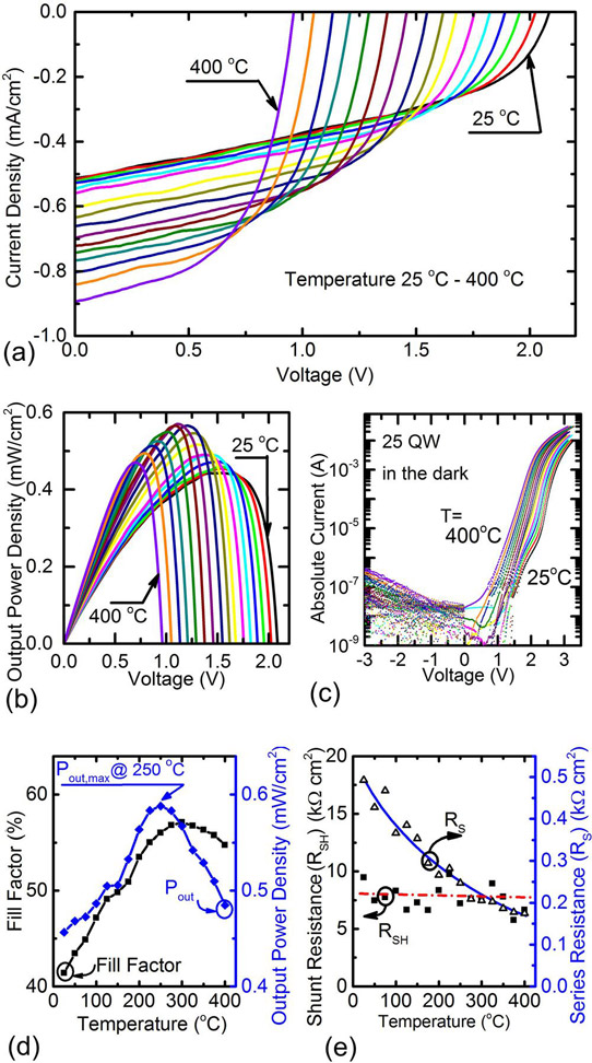
Figure 2: Junction current-voltage performance under elevated chuck temperature up to 400°C (25 QW structure) under illumination (a) and in the dark (c). (b) Output power density versus voltage, (d) fill factor and maximum output power density as functions of temperature, and (e) series resistance and shunt resistance all as functions of temperature.
The 25-well structure was also tested for performance at temperatures up to 400°C (Figure 2, Table 2). The higher temperature increases JSC at the cost of reducing VOC. The peak output power density of 0.59mW/cm2 occurred at 250°C. The fill factor increased to 57.1% at 300°C.
Table 2: Performance of 25-well device at 25°C and 400°C.
| 25°C | 400°C | |
| VOC | 2.08V | 0.96V |
| JSC | 0.51mA/cm2 | 0.89mA/cm2 |
| Pout,max | 0.46mW/cm2 | 0.48mW/cm2 |
| FF | 43.4% | 56.2% |
The improved output power and fill factor at higher temperatures is attributed to a temperature-induced shift of the cell sensitivity to longer wavelengths where there is more solar radiation. However, the maximum power at 250° compares with previous work by others where the maximum occurred at 70°C.
http://dx.doi.org/10.1063/1.4904717
The author Mike Cooke is a freelance technology journalist who has worked in the semiconductor and advanced technology sectors since 1997.


