


- News
26 January 2015
Plasma-assisted molecular beam epitaxy of indium gallium nitride
National Tsing Hua University, Taiwan, has been developing plasma-assisted molecular beam epitaxy (PAMBE) of indium gallium nitride (InGaN) for green light emission [W. C. Yang et al, J. Appl. Phys., vol117, p015306, 2015].
Improving the green emission of InGaN is a strategic aim of many researchers for creating high-quality white and colored light in equipment based on light-emitting diodes and laser diodes. Green light falls in the wavelength range 495-570nm.
Single quantum wells of InGaN sandwiched between GaN barriers were produced on GaN templates. The well was of the order 3nm thick, sandwiched between a 300nm GaN buffer and a 45nm GaN cap.
The InGaN layer was grown in two steps (Figure 1). First, all three species – In, Ga, N – were available, resulting in InGaN with 10% indium and a couple of monolayers of accumulated In atoms. The V/III flux ratio was 1 and the In/Ga flux ratio was 1.33. The indium source was then shut off and the residual indium atoms were incorporated in the remainder of the InGaN layer with up to 30% indium incorporation, dependent on growth temperature. The InGaN compositions were determined by secondary-ion mass spectroscopy (SIMS) and x-ray diffraction analysis.
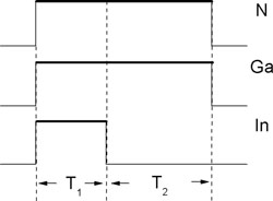 Figure 1: Scheme of source shutter sequences used in two-step PAMBE growth of InGaN SQWs.
The templates were produced on 2-inch patterned sapphire substrates (PSS) to improve crystal quality. The researchers used a Veeco MBE system with nitrogen RF plasma source, and In and Ga effusion cells. The growth mode of PAMBE InGaN has been found to be liquid- rather than vapor-phase epitaxy. Liquid Ga mixed with In and N accumulates on the surface of the substrate during epitaxial growth.
The back-sides of the substrates were coated with 1μm of titanium to give uniform, efficient heat transfer from the substrate heater. The templates were degreased before loading in the MBE system.
Before deposition the substrates were heated to 830°C in the reactor for thermal cleaning. The main deposition was carried out at 600-750°C. The growth rate was affected by the partial pressures of the In/Ga in the system. Most of the samples were processed at a "moderate growth rate" of 3.6nm/minute. However, four samples were grown at a higher rate of 5.6nm/minute.
The researchers found that increasing the growth temperature initially increased the indium content of the wells, increasing the photoluminescence (PL) wavelength toward the green region of the visible spectrum (Figure 2). However, beyond a certain point (~650°C), the indium atoms begin to evaporate from the liquid layer from which the crystal grows, saturating incorporation and the wavelength increase.
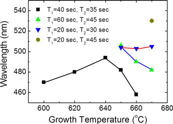 Figure 2: Trend of achieved PL wavelength for all samples grown under various growth conditions. Samples grown at a moderate rate of ~3.6 nm/min, square and triangle; faster rate of ~5.5 nm/min, circle and inverted triangle.
As indium content increases, InN becomes immiscible in GaN and phase separation occurs. The wells in high-indium-content samples were thicker (~4.5nm), leading to quantum-confined Stark effects from electric fields across the well, reducing emission intensity. The researchers therefore view 650°C as the optimal growth temperature. Also, the moderate growth rate of 3.6nm/minute is preferred.
They suggest "one way to extend the emission peak wavelength while maintaining a high emission intensity of the InGaN SQW is to minimize polarization effects by using non-polar substrates while increasing the SQW thickness."
Table 1: Indium accumulation time (T1), indium incorporation time (T2), and growth temperature (TG) used to grow InGaN/GaN SQW samples and their PL peak wavelengths, relative intensities, and indium content. All samples were grown at ~3.6 nm/min, except samples N, O, P, and Q, at ~5.5 nm/min.
| Sample | T1 (s) | T2 (s) | TG (°C) | PL peak wavelength (nm) | Relative PL intensity (a.u.) | In content (%) |
| A | 40 | 25 | 600 | 460 | 5.11 | … |
| B | 40 | 35 | 600 | 470 | 2.41 | 17.8 |
| C | 40 | 45 | 600 | 500 | 2.22 | … |
| D | 40 | 35 | 620 | 480 | 3.36 | 22.5 |
| E | 40 | 35 | 640 | 494 | 3.44 | 28.1 |
| F | 40 | 35 | 650 | 482 | 8.26 | 23.1 |
| G | 40 | 35 | 660 | 458 | 8.67 | 12.2 |
| H | 40 | 45 | 640 | 500 | 5.23 | … |
| I | 40 | 45 | 650 | 480 | 8.12 | … |
| J | 40 | 60 | 640 | 516 | 3.03 | 28.6 |
| K | 60 | 45 | 650 | 506 | 10.53 | 30.2 |
| L | 60 | 45 | 660 | 490 | 8.88 | … |
| M | 60 | 45 | 670 | 480 | 11.63 | … |
| N | 20 | 30 | 650 | 504 | 6.1 | … |
| O | 20 | 30 | 660 | 503 | 10.7 | … |
| P | 20 | 30 | 670 | 505 | 8.4 | 31.8 |
| Q | 20 | 45 | 670 | 530 | 1.2 | 32 |
The longest wavelength with strong PL emission was achieved with 30% indium content and 506nm wavelength (Table 1).
http://dx.doi.org/10.1063/1.4905419
The author Mike Cooke is a freelance technology journalist who has worked in the semiconductor and advanced technology sectors since 1997.


