


- News
23 January 2015
Electrical injection of rolled-up heterostructure lasers
McGill University in Canada claims to have created the first electrically injected rolled-up semiconductor tube laser [M. H. T. Dastjerdi et al, Appl. Phys. Lett., vol106, p021114, 2015]. Although rolled-up heterostructure lasers have been achieved using optical pumping, the researchers say that electrically injected rolled-up semiconductor tube lasers have not previously been reported.
Rolled-up heterostructures are grown with a strain profile that causes the material to roll up when released from the growth substrate. Rolled-up semiconductor tubes can be used to create laser cavities with ultra-high-quality (Q) factors (i.e. low loss), directional emission, and controlled polarization.
The McGill electrically injected device could lead the way to coherent light sources for applications in chip-level optical communications. The researchers also believe that the device can be integrated into a silicon platform without performance degradation.
The heterostructure (Figure 1) was grown on indium phosphide (InP) using molecular beam epitaxy (MBE). The structure was coherently strained so that it would roll up when released from the InP growth substrate. The light emission was from two quantum wells of indium gallium arsenide (In0.53Ga0.47As). The structure's photoluminescence (PL) peak was at 1.57μm wavelength. Optical communications are often based on wavelengths around 1.5μm.
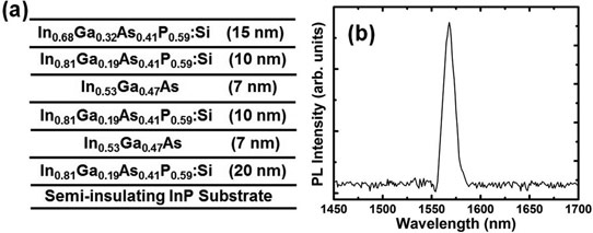
Figure 1: (a) Schematic of coherently strained InGaAs/InGaAsP quantum well heterostructures grown on semi-insulating InP substrate. (b) PL spectrum measured at room temperature.
Silicon doping during heterostructure growth created n-type conductivity with negative charge electron carriers. Hole carriers were achieved with ion implantation with beryllium p-type doping of part of a U-shaped mesa region around the tube structure (Figure 2). The p-type doping was thermally activated at ~600°C for 35 seconds. Out-diffusion of arsenic and phosphorus atoms during activation was avoided by depositing 40nm of silicon nitride.
Nickel/germanium/gold and palladium/titanium/palladium/gold were used as the n- and p-type metal contacts, respectively. The contacts were annealed at 400°C for 1 minute.
Various wet etches were used to create the U-shaped mesas and to under-cut the heterostructure so that it would release and curl up into tubes. The resulting devices were 100μm long with 140nm wall thickness. The tube diameter was 5μm.
The researchers comment: "Shown in Figure 2(d), the presence of corrugations on the tube surface can be clearly identified, which provide strong optical confinement along the tube axial direction. The controlled surface geometry was defined by the corrugations introduced at the inner edge of the U-shaped mesa."
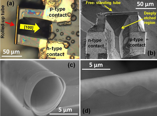
Figure 2: (a) Optical microscopy image of free-standing rolled-up tube device with n- and p-metal contacts on either side. (b) SEM of fabricated tube device with n- and p-metal contacts. (c) SEM side view of tube cavity. (d) SEM of free-standing part of tube device showing surface corrugations for axial mode confinement.
The turn-on voltage of 3V at 80K is described by the researchers as 'relatively high'. Limitations in the p-dopant activation annealing step are blamed. Proper activation would require higher temperatures of 800-900°C, but then the heterostructure would not roll up properly. "This is probably due to alterations in the crystalline structure of the strained bilayer at temperatures significantly higher than the growth temperature of the device heterostructure," the researchers write.
The 80K laser threshold current for a mode at 1485nm was 1.05mA, where the full-width at half-maximum (FWHM) reduced to 2nm from 3.3nm subthreshold. The FWHM increased at higher currents due to self-heating effects. The other modes of the device did not show any lasing effect.
The Purcell factor of the enhancement over the spontaneous emission rate in the cavity was estimated to be 4.3, based on a quality (Q) factor of 800, effective mode volume of 4μm3, and effective refractive index of 2.26.
Optical communications Heterostructure lasers InP InP growth substrate InGaAs MBE
http://dx.doi.org/10.1063/1.4906238
The author Mike Cooke is a freelance technology journalist who has worked in the semiconductor and advanced technology sectors since 1997.


