


- News
16 January 2015
FBH uses LayTec's EpiCurve in-situ metrology to eliminate SiC/GaN wafer cracking in ICP etching
In-situ metrology system maker LayTec AG of Berlin, Germany says that researchers at Berlin-based Ferdinand-Braun-Institut für Höchstfrequenztechnik (FBH) have applied EpiCurve in-situ metrology for optimizing etching recipes in a Sentech SI 500 inductively coupled plasma reactive-ion etch (ICP-RIE) tool.
With standard etching recipes the SiC/GaN wafer (pasted to a glass or sapphire carrier) frequently cracks because it suffers from a ±50μm wafer bow due to vertical temperature gradients and differences in the thermal expansion coefficients of carrier, substrate and GaN.
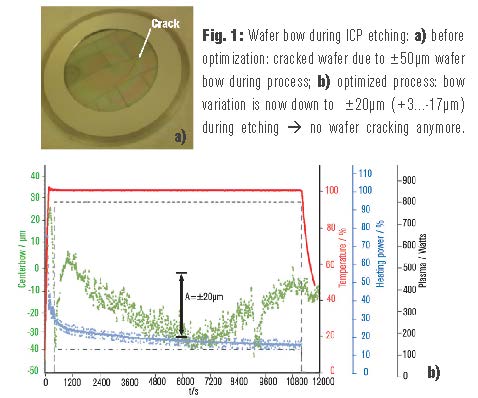
By using EpiCurve in-situ strain engineering, the wafer bow was reduced to ±20μm (see Figure) and wafer cracking can be completely avoided, says the firm.
A presentation of the research can be downloaded using the following link:
www.laytec.de/fileadmin/Editor_Uploads/Marketing/PDFs/


